
A comprehensive technical synthesis for hardware engineering and procurement excellence.
This article synthesizes datasheet parameters and empirical performance checks so engineers can assess the 06035A560KAT quickly and confidently. It combines a part-number decode, a checklist of definitive specs to extract, recommended lab tests (DC-bias, frequency response, ESR), design and assembly guidance, and an incoming inspection/procurement checklist. Target audience: US hardware engineers who need data-forward, reproducible steps. Expected read: ~10 minutes.
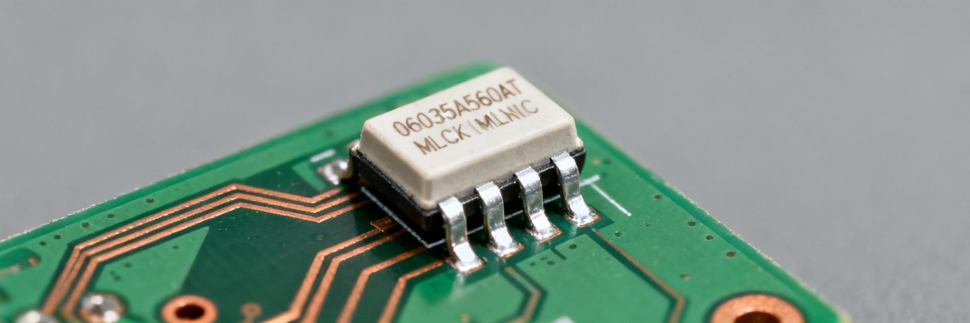
Figure 1: Typical 0603 Package Geometry and Internal Structure
Background: Decoding 06035A560KAT and Where to Start
How to read the part number: size, capacitance code, tolerance, dielectric family
MLCC part numbers are tokenized: package size, nominal capacitance code, tolerance letter, rated voltage and dielectric series. For example, the token matching 0603 indicates package geometry (1.6mm x 0.8mm); capacitance codes map to pF values per the manufacturer table; K usually denotes ±10% tolerance. Always cross-check each token against the official datasheet fields rather than assuming industry conventions.
Datasheet fields to extract immediately (must-have specs)
Capture nominal capacitance, tolerance, rated voltage, package dimensions, dielectric family/class, temperature coefficient, DC-bias characteristic, allowable ripple/current if given, life and temp test outcomes, recommended solder profile and land pattern. Note differences between commercial and automotive grades—look for longer life-test hours, tighter IR requirements, and AEC-style qualifications.
Technical Specs: How to Present a Complete, Usable Specs Table
| Field | Value | Units / Notes |
|---|---|---|
| Part Number | 06035A560KAT | Standard PN |
| Nominal Capacitance | 56 | pF |
| Tolerance | ±10% | K-Code |
| Rated Voltage | 50 | VDC |
| Dielectric Class | C0G (NP0) | Ultra-stable |
| Dimensions | 1.60 x 0.81 | mm (0603 Imperial) |
Performance Summary: Measurement Methods & Typical Plots
Engineers should perform DC-bias sweeps and frequency sweeps. Below is a visualization of typical C0G vs X7R stability performance under voltage stress, highlighting the superiority of the 560KAT’s dielectric class.
Note: C0G dielectrics maintain near-perfect capacitance across the full voltage range.
How to present results: recommended charts and interpretation tips
Include: capacitance vs DC bias (% of nominal vs applied V), capacitance vs frequency, impedance magnitude/phase and ESR vs frequency, and temperature drift plots. Interpretations: large DC-bias drops reduce decoupling effectiveness; high DF at operating frequency indicates heat and loss; resonant behavior informs RF suitability. Flag alarm signs explicitly in captions.
Design & Application Guidance for US Engineers
Selection & Placement
Derate based on dielectric: for high-κ types, plan 20–50% loss; for stable C0G like the 560KAT, select minimal derating. Place decouplers close to power pins with shortest vias and low-inductance planes. Adjust land pattern fillets to reduce tombstoning on 0603 parts.
Assembly Considerations
Follow manufacturer reflow profiles. Watch for board flex—MLCC cracks often originate from mechanical stress. Use X-ray for internal cracks and automated optical inspection (AOI) post-reflow for high-reliability boards.
Applications, Alternatives & Procurement Checklist
- ✓ Typical Applications: High-frequency bypass, timing circuits, and RF matching where C0G stability is critical.
- ✓ Procurement: Request full datasheet, lot-level test reports, and sample test plans. Ensure lot traceability.
- ✓ Incoming Inspection: Visual ID, dimensional check, and capacitance spot check at 1 kHz.
Summary
This workflow gives a clear path from decoding the 06035A560KAT part number to extracting essential electrical and mechanical specs, executing reproducible DC-bias and frequency-sweep tests, and enforcing pragmatic design, assembly, and procurement checks. Key actions: populate the quick-reference specs table from the official datasheet, run a DC-bias sweep and impedance analysis before committing to a dielectric choice, apply derating and footprint tweaks to reduce tombstoning and cracking, and enforce incoming inspection with lot-level verification. Use the recommended figures—capacitance vs voltage, impedance/ESR vs frequency, and temperature-drift plots—to inform PCB decoupling and RF decisions. Before production release, validate a representative sample on the intended assembly and attach raw measurement files to the procurement lot for traceability.
Key Summary Points
- Decode tokens: Prevent misinterpretation of the 06035A560KAT mapping.
- Data Logging: Report cap vs voltage and ESR with raw data and uncertainty.
- Layout: Apply dielectric-specific derating and footprint adjustments.
- Quality: Require bias curves and lot test reports before acceptance.

