
Vendor datasheets consistently list Capacitance, Tolerance, Vr, DF, ESR/IR, SRF/ESL, and land patterns.
Use these parameters as primary filters before bench validation to avoid production surprises.
Quick Specs at a Glance
Electrical Baseline
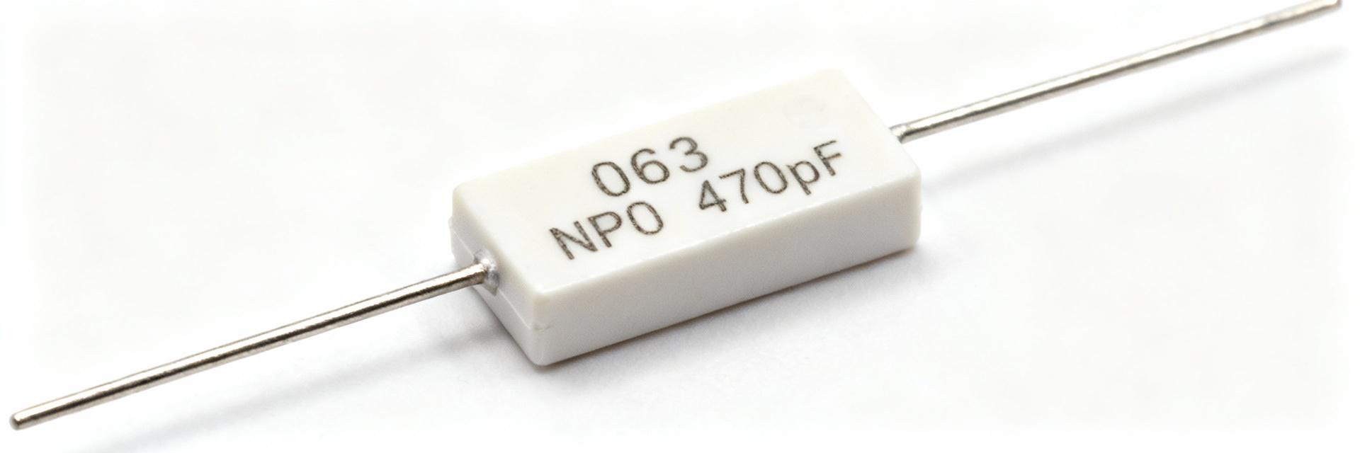
- Capacitance: 470 pF nominal value.
- Voltage Rating: Range of 16 V – 100 V (Choose Vr ≥ DC + transients).
- Dielectric: NP0/C0G (~±30 ppm/°C near-zero drift).
- Losses: Controlled Dissipation Factor (DF) and high Insulation Resistance (IR).
- RF Metrics: Typical SRF in hundreds of MHz; layout-dependent ESL.
Physical & Mechanical
- Package: 0603 Imperial (1608 Metric).
- Termination: Ni barrier or Ag finishes; confirm solderability.
- Assembly: Follow standard reflow profiles and MSL guidelines.
- Mechanical: High resistance to board flex and thermal shock.
Electrical Performance & Behavior
NP0 provides superior stability over temperature and frequency compared with high-K dielectrics like X7R.
| Parameter | NP0 (C0G) Characteristic | Design Impact |
|---|---|---|
| Temp. Coefficient | ±30 ppm/°C | ≈0.54% change from –55°C to +125°C |
| DC Bias Effect | Negligible ( | Maintains nominal C and Q under load |
| Aging | 0% per decade hour | Long-term frequency stability |
Stability Visualization (NP0 vs. X7R)
Selection Checklist & Methods
- ✓ Capacitance & tolerance at specified test frequency.
- ✓ Voltage rating with safety margin (Vr ≥ DC + transients).
- ✓ Verify SRF/ESL for RF applications.
- ✓ Mechanical land pattern compatibility with 0603 footprint.
- ✓ Soldering profile and MSL classification compliance.
PCB Layout & Reliability
Board-level parasitics often dominate real-world behavior. Follow these guidelines:
Trace Optimization
Minimize trace length and use multiple ground vias to reduce effective ESL and raise SRF.
Pad Dimensions
Standard 0603 footprint (≈0.9mm x 0.6mm). Adjust based on specific manufacturer land patterns.
Thermal Stress
Adhere to reflow profiles to prevent body cracking or tombstoning during assembly.
Summary
Verify core electrical specs (470 pF, tolerance, voltage rating), NP0 tempco and low DC bias behavior, SRF/ESL for RF, correct 0603 land pattern and reflow limits, and perform LCR/temperature/DC-bias validation before production; a disciplined checklist avoids costly spin cycles.
- Confirm 470 pF nominal and tolerance.
- Ensure Vr includes transients.
- Verify SRF for GHz applications.
- Validate samples under thermal sweep.

