
0566-2-15-15-21-27-10-0 Full Specifications & Pin Data Report
The 0566-2-15-15-21-27-10-0 serves as a high-precision technical reference for engineers. Key parameters include an accepted lead diameter range of 0.015–0.022 in (0.38–0.56 mm), a pin hole diameter of ≈0.031 in (0.79 mm), and a mounting hole diameter of ≈0.039 in (0.99 mm). This report consolidates critical dimensions, PCB footprint guidance, and soldering protocols to ensure consistency across design reviews and procurement inspections.
Product Overview
Functional Scope
This component is a precision pin receptacle designed to accept plated wire leads within a strictly defined diameter band. Featuring a no-tail, solder-mount configuration with a small flange, it is ideal for low-current signal connectors, test-fixture sockets, and PCB-mounted receptacles where vertical space is at a premium.
Part-Number Anatomy
The complex alphanumeric sequence 0566-2-15-15-21-27-10-0 encodes essential data regarding series, contact geometry, and plating options. Understanding this segmenting helps engineers identify dimensional drawings and alternate configurations for search queries like "0566 part pin hole diameter" or "0566-2 series plating options."
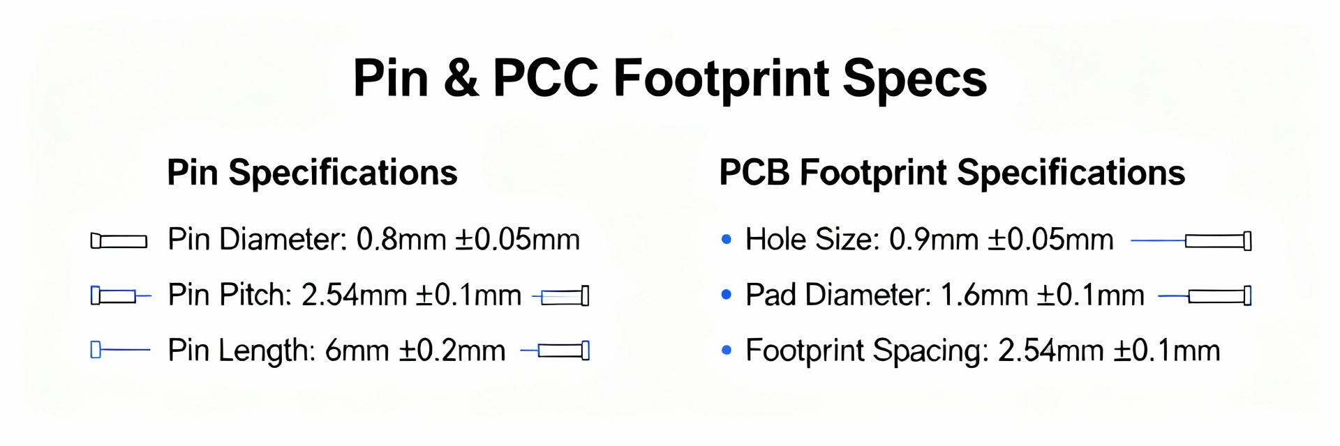
Mechanical Specifications & Dimensional Data
Dimensional Visual Analysis (inch)
| Parameter | Value | Units | Tolerance | Notes |
|---|---|---|---|---|
| Accepted lead diameter | 0.015–0.022 (0.38–0.56) | in / mm | ±0.0015 (±0.04) | Critical for mating reliability |
| Pin hole diameter | 0.031 (0.79) | in / mm | ±0.002 (±0.05) | Drill size reference |
| Mounting hole diameter | 0.039 (0.99) | in / mm | ±0.002 (±0.05) | Through-hole clearance |
| Flange diameter | 0.058 (1.47) | in / mm | ±0.003 (±0.08) | Pad annulus sizing |
| Overall length | 0.138 (3.51) | in / mm | ±0.004 (±0.10) | Seating height for stackup |
Electrical Performance
Key electrical metrics define signal integrity. Maximum current capacity, contact resistance (mΩ), and voltage rating must be confirmed against the contact geometry and plating material. Using high-conductivity plating reduces resistance, which is vital for minimizing signal loss in low-voltage paths.
Environmental Reliability
Operating temperature ranges and soldering windows govern long-term reliability. Engineers should reference test standards for mechanical shock, thermal cycling, and salt spray. Ensure that reflow profiles (peak temperature and duration) align with supplier-specified limits.
PCB Mounting & Soldering Guidelines
Footprint Strategy
- • Use a ≈0.039 in (0.99 mm) drill for the mounting hole.
- • Ensure a pad ≥0.150 in (3.81 mm) annular ring to support flange seating.
- • Maintain keepout zones to ensure mechanical engagement and prevent electrical shorts.
Process Controls
Wave, selective, and manual soldering are approved. It is imperative to control peak temperatures per lead-free profiles. Post-solder inspection should quantify wetting, fillet shape, and void acceptance, followed by mechanical retention tests to verify the integrity of the board interface.
Integration & Quality Assurance
Troubleshooting Checklist
Key Summary
- [✓] Accepted lead diameter: 0.015–0.022 in (0.38–0.56 mm) — critical for mating; verify during incoming inspection.
- [✓] PCB Footprint: Mounting hole Ø 0.039 in (0.99 mm) and flange Ø 0.058 in (1.47 mm) are required drill/pad dimensions.
- [✓] Mechanical Fit: Pin hole Ø 0.031 in (0.79 mm) and length 0.138 in (3.51 mm) are nominal; confirm supplier tolerances.
- [✓] Data Reporting: Ensure test reports for max current, dielectric strength, and mechanical life are requested.

