
Common failures such as misfit, wrong pin mapping, or broken mounting tabs create expensive rework. This guide presents a concise, repeatable verification workflow to avoid those risks when validating a PCB footprint.
Objective
The workflow covers datasheet extraction, mechanical and electrical checks, and a case-specific walkthrough so engineers can confidently verify 051-24-1040 footprints before production.
Expectations
Expect a clear checklist, practical CAD checks, and low-cost fit tests that reduce assembly failure and scrap. The outcome is a verifiable sign-off path.
Background: Why verifying a PCB footprint matters
What a PCB footprint actually includes
Point: A footprint is more than pads — it is the physical contract between PCB and part.
Evidence: Typical footprints include pads, drill holes or slots, courtyard, silkscreen, assembly origin, and a 3D body.
Explanation: Each element affects fit, solderability, and assembly: pads control solder fillet, drill holes and annular rings determine mechanical strength, courtyard avoids collisions, and the 3D model reveals mechanical clashes.
Common failure modes
Point: Connectors and through-hole parts suffer repeatable failure patterns that are avoidable.
Evidence: Common issues are wrong pitch, incorrect hole or slot shape, misplaced mounting tabs, and insufficient edge clearance.
Explanation: These failures cause mechanical looseness, misalignment, or wave-solder bridging; a single misplaced mounting tab can force costly board rework.
Gather the right component data: datasheet & mechanical drawing checks
Critical dimensions and callouts to extract
Point: Start by extracting explicit callouts from the datasheet.
Evidence: Copy pin count and numbering, pitch, row spacing, hole types (round or slot), tab dimensions, and tolerances.
Explanation: Capturing these fields verbatim prevents interpretation errors and creates a traceable source for footprint decisions and assembler notes.
Translate tolerances into PCB values
Point: Convert nominal dimensions into worst-case PCB values with fab allowances.
Evidence: Translate nominal hole size to worst-case considering drill tolerance; choose pad oversize to maintain annular ring.
Explanation: Add 4–6 mils for drill tolerance on plated through holes, and always confirm the fabricator’s published capabilities before finalizing values.
Verification Parameter Matrix
Mechanical Verification
- ✔ Pads & Drills: Inspect pad-to-drill alignment and use layer isolation to confirm minimum annular rings.
- ✔ Courtyard: Ensure assembly and tooling clearance for mating hardware travel and handling.
Electrical & Assembly
- ⚡ Pin Mapping: Run a netlist compare and perform a visual rotation/mirror check with the 3D body.
- ⚡ Solder Mask: Size paste apertures per pad geometry and add thermal reliefs for large copper pours.
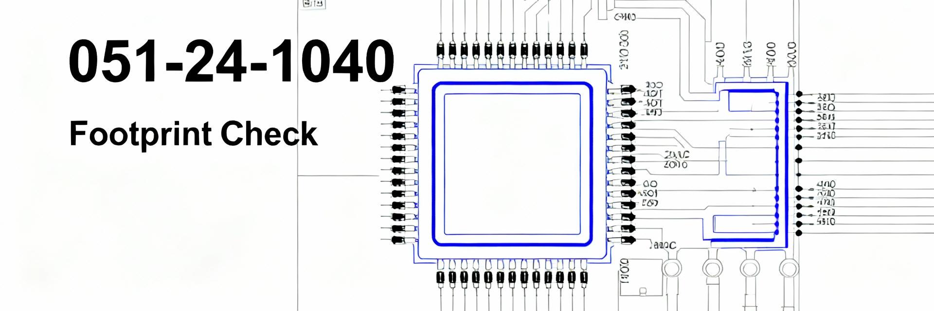
051-24-1040 Verification Walkthrough
Datasheet Cross-Check List
Create a component-specific checklist for 051-24-1040 and paste datasheet callouts into your review document. Confirm pin count, pitch, and anchor/tab hole shapes. Copy the exact datasheet dimension lines into the checklist and flag any missing callouts for supplier clarification.
Fit & Assembly Tests
Validate fit with low-cost physical tests. Place the 3D model in CAD, export a 1:1 paper template, and assemble a single-part prototype. These checks catch interference and misoriented tabs that DRC might miss.
Summary
Verifying a PCB footprint early prevents fit and assembly failures and saves cost. Apply these standard steps:
- Extract and document datasheet callouts for the 051-24-1040: pin mapping, hole/slot dimensions, and tab plating.
- Perform mechanical checks in CAD: validate pad/drill sizes, annular ring, and courtyard clearances.
- Run electrical checks: map pins to the schematic and validate orientation with a 3D model before sign-off.

