06035C103KAT2A性能报告:电容和可靠性

摘要:受控测试活动的测量结果显示,在加速应力下,DC 偏压电容有所降低,温度依赖性适中,且失效发生率较低但可测量。 证据 测试的器件在 DC 偏压下表现出平均电容漂移,在长时间高温偏置暴露后有较小的百分比变化。 解释 本报告总结了客观的电容性能和以可靠性为导向的指南,旨在为工程师提供设计和采购决策依据。 组件概览与基准规格 关键电气和机械规格 基准规格和测试设置项对于可重复的解释至关重要。标称电容 10 nF,容差 ±10%,额定电压 50 V,介质类别 X7R,封装尺寸 0603,工作温度 −55 °C 至 +125 °C。 规格项 目标值 数据来源 器件型号 06035C103KAT2A 数据表 / 测量值 标称电容 10 nF 数据表 容差 ±10% 数据表 额定电压 50 V 数据表 介质 / 封装 X7R / 0603 数据表 工作范围 −55 °C 至 +125 °C 数据表 电容性能:DC 偏压、温度和老化 DC 偏压与电压系数分析 通过标准化的 V-步进测试量化电容随施加 DC 偏压的变化。设计人员应预料到偏压引起的电容降低(额定电压下典型范围为 10–30%)。 偏置 (V) 平均 C (nF) 变化百分比 010.0 ±0.30% 109.1 ±0.4−9% 258.2 ±0.5−18% 50 (额定)7.0 ±0.6−30% 可视化 50V 下的电容保持率 0% 保持率 70% 保持率 (30% 损失) 温度依赖性与时间老化 区分可逆温度系数与不可逆老化。预期 X7R 在不同温度下会出现可逆偏移,但在偏置应力下会出现逐渐的不可逆下降(1000 小时内下降 1–5%)。 可靠性测试与失效模式 测试类型 条件 样本量 (n) 失效数 HTRB / HTB 125 °C, 50 V, 1000 小时 77 1 (1.3%) THB 85 °C / 85% RH, 通电, 1000 小时 50 0 温度循环 −55 / +125 °C, 1000 个循环 50 2 (4.0%) 根本原因分析: 典型观察结果包括可见裂纹、开路/短路以及 ESR 增加。开裂通常与组装过程中的 PCB 应力或热膨胀有关。 比较基准:同类 0603 X7R MLCC 器件类别 0 V 下的 C (nF) 50 V 下的 %Δ +125 °C 下的 %Δ 1000h HTB 失效 测试对象 (06035C103KAT2A) 10.0 −30% −6% 1/77 同类产品 A 10.0 −22% −4% 0/77 同类产品 B 9.8 −35% −7% 3/77 行动建议 PCB 设计与降额 电压降额: 在偏置敏感型设计中,目标电压 ≤25 V(额定值的 50%),以保持电容。 布局: 避免板边或弯曲区域;放置在实心板区域以减少开裂。 焊盘几何形状: 使用完整的焊点圆角和制造商推荐的焊盘图案。 质量保证与进料检验 可追溯性: 要求批次报告和可追溯性文件。 抽检: 对进料批次进行电容随偏压变化的检查。 外观/CT: 针对机械缺陷、空洞或预存裂纹进行采样。 最终总结 在典型应用中,06035C103KAT2A 符合常见 MLCC 电容器对温度稳定性的预期,但表现出中等的 DC 偏压电容降低。设计人员必须应用降额规则并确保精确的 PCB 布局,以维持长期可靠性。 ✔ 降额至 50% ✔ HTRB 抽检 ✔ 无应力布局 常见问题解答:06035C103KAT2A 的性能与可靠性 我应该预期的 DC 偏压电容变化量是多少? 典型的 X7R 0603 器件在额定电压下可能显示 10–35% 的降幅;本次活动中的测量平均值显示在 50 V 时约为 −30%。设计人员应使用特定样品的测量值来制定降额策略。 哪些加速测试最能预测现场失效? HTRB/HTB(带偏置的高温测试)和 THB(带电的湿度测试)最能预测电气退化;温度循环和机械冲击则能揭示开裂敏感性。 建议的进料检验阈值是多少? 如果 0 V 下的电容在 ±10% 以内,且额定电压下的偏压损失为

2026-01-29 21:13:11

470 pF 0603 NP0电容器-完整规格和数据表

分销商列表和元器件目录显示了数十种 470 pF 0603 NP0 零件,其常见电压额定值从 16 V 到 100 V 不等,公差从 0.5% 到 5%。这份紧凑的数据驱动指南重点介绍了精密射频(RF)和定时电路所需的电气、物理及特定应用规格。 核心要点 正确选择平衡了电气稳定性和板级寄生效应,以确保长期可靠性。 证据 供应商数据手册一致列出了电容量、公差、Vr、DF、ESR/IR、SRF/ESL 和焊盘图形。 策略 在工作台验证之前使用这些参数作为主要过滤条件,以避免生产意外。 规格一览 电气基准 电容量: 470 pF 标称值。 额定电压: 范围 16 V – 100 V(选择 Vr ≥ 直流电压 + 瞬态电压)。 介电材料: NP0/C0G(~±30 ppm/°C 接近零漂移)。 损耗: 受控的损耗因数 (DF) 和高绝缘电阻 (IR)。 射频指标: 典型的自谐振频率 (SRF) 为数百 MHz;等效串联电感 (ESL) 取决于布局。 物理与机械 封装: 0603 英制 (1608 公制)。 端电极: 镍阻挡层或银饰面;确认可焊性。 组装: 遵循标准回流焊曲线和 MSL 指南。 机械性能: 高抗电路板弯曲和热冲击能力。 电气性能与行为 与 X7R 等高 K 介电材料相比,NP0 在温度和频率方面提供了卓越的稳定性。 参数 NP0 (C0G) 特性 设计影响 温度系数 ±30 ppm/°C 在 –55°C 至 +125°C 之间约变化 0.54% 直流偏置效应 可忽略不计 在负载下保持标称 C 和 Q 老化 每十倍小时 0% 长期频率稳定性 稳定性可视化 (NP0 vs. X7R) NP0 稳定性 99% X7R 稳定性 ~75% 选择清单与方法 ✓ 指定测试频率下的电容量和公差。 ✓ 具有安全裕度的额定电压 (Vr ≥ DC + 瞬态)。 ✓ 验证射频应用的 SRF/ESL。 ✓ 机械焊盘图形与 0603 封装的兼容性。 ✓ 焊接曲线和 MSL 分类合规性。 PCB 布局与可靠性 板级寄生效应通常主导实际表现。请遵循以下准则: 走线优化 最小化走线长度并使用多个接地过孔,以减少有效 ESL 并提高 SRF。 焊盘尺寸 标准 0603 封装(≈0.9mm x 0.6mm)。根据特定制造商的焊盘图形进行调整。 热应力 遵守回流焊曲线,防止组装过程中出现本体开裂或立碑现象。 总结 在生产前验证核心电气规格(470 pF、公差、额定电压)、NP0 温度系数和低直流偏置行为、射频 SRF/ESL、正确的 0603 焊盘图形和回流焊限制,并进行 LCR/温度/直流偏置验证;严格的清单可以避免昂贵的返工周期。 确认 470 pF 标称值和公差。 确保 Vr 包含瞬态电压。 验证 GHz 应用的 SRF。 在热扫描下验证样品。 常见问题 在射频频率下,470 pF 0603 NP0 电容器与 X7R 相比如何? + NP0 的温度和直流偏置敏感性比 X7R 低得多,且损耗因数 (DF) 通常也更低,因此在射频频段具有更稳定的电容量和更高的品质因数 (Q)。预计 NP0 在正常温度范围内的电容量偏移低于 1%,而 X7R 的偏移可能超过 10%,并带有会降低匹配性能的偏置相关损耗。 对于精密定时应用,我应该验证什么? + 在相关测试频率下确认标称电容量 C 和公差、带有电容量 vs 温度图表的 NP0 温度系数(例如 ±30 ppm/°C)、老化信息以及带有推荐焊盘图形的机械图纸。如果振荡器稳定性至关重要,请索取样品测试数据。 哪些工作台测试可以验证 470 pF 0603 NP0 电容器的射频用途? + 在工作频率下进行 LCR 测量,进行直流偏置测试以量化电压系数,并进行热箱扫描。在安装到代表性 PCB 焊盘的零件上进行网络分析仪扫描,对于捕获实际寄生效应至关重要。

2026-01-29 21:05:53

06035A220KAT电容器规格报告:C0G,50V,22pF

导言:06035A220KAT 是一款紧凑型 0603 封装 MLCC,标称电容量为 22 pF,额定电压为 50 VDC,采用 C0G 介质——这是针对精密定时、射频 (RF) 和模拟前端设计的理想选择。C0G 提供近乎零的温度系数 (~0 ±30 ppm/°C) 和极低的介质损耗(损耗因数通常 <0.1%),因此本报告重点关注工程师可直接应用的实用电容器规格及测试/选型指南。 本报告采用面向测量的指南:包括数据手册验证要点、环境行为表现以及工作台验证步骤。 背景:了解 06035A220KAT 及其市场定位 观点:解读标识并确定该器件在产品系列中的位置。证据:典型的 MLCC 零件代码包含了封装、电容量代码、容差、电压和系列信息。解释:设计人员应将印制代码视为简写——务必交叉核对数据手册以进行准确对应,因为供应商的系列后缀各不相同。 零件代码分解与物理封装 0603:封装尺寸(英制 0603,标称封装尺寸 ≈ 0.06" × 0.03"); 220:代表 22 pF 的电容量代码; K:容差标识(通常为 ±10%); 50 V:额定直流工作电压(在数据手册中有明确说明); C0G:介质类别(稳定性和损耗特性)。 介质概述:C0G (NP0) 特性 C0G 为精密应用提供了最稳定的 MLCC 介质,表现出约 0 ±30 ppm/°C 的温度系数且老化效应微乎其微。 电容量稳定性 (C0G)99.9% 电容量稳定性 (X7R)85% 详细电气规格与性能数据 精简的规格表整合了设计人员在选型前需核实的电容器关键规格,以减少错误并支持采购比价。 参数 典型值 / 目标值 电容量 22 pF 容差 ±10% (K) — 核实标识 额定电压 50 VDC 介质 C0G (NP0) 损耗因数 (DF) 绝缘电阻 高 — 数据手册列出了 µA 或 GΩ 规格 SRF (自谐振频率) 数百 MHz 到低 GHz 范围 * SEO 提示:在采购数据手册中包含“电容器规格”。 测量与验证:工作台测试流程 建议设置 工具:精密 LCR 表、阻抗分析仪。 条件:1 kHz 下的小信号交流电以及目标射频频率。 校准:必须进行开路/短路/负载补偿。 “ 测试流程: 1. 校准夹具(开路/短路/负载)。2. 在 1 kHz 下测量 C 和 DF,然后扫频至射频频段。3. 在额定电压下测量漏电流/绝缘电阻。4. 记录温度;如需进行热评估则重复上述步骤。 典型应用与使用场景选型 最适合的应用 精密定时网络 振荡器调谐(低漂移) 射频匹配与滤波 ADC 前端 / 采样保持 设计可靠性 采用保守的设计余量。使用适度的电压降额,并核实回流焊温度曲线的兼容性,以避免机械应力失效。 采购、替代件与实施 最终实施核查表 ✔ 确认封装和焊盘图案 (IPC) ✔ 核实回流焊温度曲线兼容性 ✔ 在采购中明确测试限制 ✔ 订购评估样品进行验证 ✔ 记录射频频段的 SRF 和 DF 总结 06035A220KAT 是一款 0603 封装的 22 pF、50 V、C0G MLCC,其电容器规格有利于在定时、射频匹配和精密模拟工作中实现稳定、低损耗的性能。设计人员在批量生产前应验证 SRF、DF 和漏电流,并进行工作台验证。 核实核心规格:22 pF, 50 V, C0G 介质。 生产前使用校准过的 LCR 表进行测量。 在代表性条件下验证 SRF 和损耗因数。 常见问题解答 — 关于选型与测试的常见问题 工程师应如何验证 0603 封装 22 pF C0G 的 SRF? + 回答:使用阻抗分析仪,在模拟 PCB 寄生效应的夹具中安装零件,从低 MHz 扫频至预期的射频频段。记录幅度和相位以定位阻抗最小值 (SRF),并在包含任何串联走线或焊盘的情况下重复测量,因为布局会使 SRF 下移。 对于定时与射频应用,哪些容差和 DF 限制是可接受的? + 回答:对于振荡器定时,容差和温度系数决定了频率精度——优选 ±5% 或更小,且具备 C0G 稳定性。对于射频匹配,低 DF( 哪些测量误区最常导致采购中的电容器规格失效? + 回答:最常见的问题是未修正夹具/引线、测试期间温度未受控,以及在远离应用频段的频率下进行测量。采购时应要求提供经夹具修正的数据和明确的测试报告,以避免后续出现意外。

2026-01-29 20:59:32

05710008L保险丝座:完整规格和数据表下载

技术库存显示,额定值接近 30 A / 600 V 的面板安装式管状保险丝座仍是工业控制面板和配电领域指定最多的组件之一。准确的规格和经过验证的数据表对于安全设计和采购至关重要。 快速概览 05710008L 是一款单极面板安装式管状保险丝座,专为工业控制面板、电机控制中心和配电组件设计。请使用标识符 “05710008L 30A 600V 保险丝座” 进行精确采购。 关键应用: 为小型保险丝(~10 mm × 38 mm)提供高可靠性保护。 规格概览 额定电流 30 A 额定电压 600 V 交流 / 直流兼容 工作温度 −40°C 最低额定值 参数 详细数值 保险丝尺寸兼容性 小型 / ~10 mm × 38 mm (13/32" × 1-1/2") 极数 1 (单极) 安装方式 面板安装 分断能力 请参阅安装的具体保险丝类别 电气性能与材料安全 电气额定值 确认连续电流额定值和交流/直流电压限制对于保护协调至关重要。数据表详细说明了 30 A 容量和 600 V 限制,这对于选择符合电机负载或通用保护电路中浪涌和短路条件的保险丝时间-电流特性至关重要。 材料与合规性 采用高级绝缘聚合物和铜合金触点(通常为镀锡或镀银)制成。这些材料确保了长期可靠性和耐腐蚀性。请务必在官方技术文件中验证 UL/IEC/CSA 认证以及 RoHS/REACH 合规性。 安装与安装最佳实践 尺寸占用空间 确保面板开孔符合指定的矩形或圆形图案。 验证面板后方的总深度间隙。 保持相邻组件之间适当的爬电距离和电气间隙。 固定检查清单 遵循安装螺钉的扭矩规格以防止接触不良。 使用推荐的终端线规以确保热稳定性。 在震动剧烈的环境中实施防转措施或使用垫圈。 典型应用案例 工业面板进线分支电路、电机启动器保护(30 A 与分支电流匹配处)以及开关柜分配。在潮湿环境中,强烈建议增加密封或使用带垫圈的开孔。 更换策略 通过参数而非仅仅通过零件编号来验证更换件。交叉引用保险丝尺寸、电流/电压额定值和机械占用空间。在采购记录中记录匹配参数,以避免假冒风险。 数据表验证行动计划 1. 内容审核 验证 PDF 中的准确零件编号、完整电气规格、机械单位(毫米/英寸)和修订代码。 2. 来源真实性 仅从原始制造商或授权经销商处获取文件,以防止灰色市场风险。 3. 可追溯性 针对关键批次或长交期项目索取符合性证明 (CoC),以便进行项目归档。 总结 及早验证: 在 BOM 发布前确认 30 A / 600 V 限制和小型保险丝兼容性。 材料检查: 在数据表中确认耐腐蚀性和阻燃等级 (RoHS/REACH)。 精准安装: 使用尺寸图和扭矩建议,避免昂贵的面板返工。 风险缓解: 记录修订代码,并要求对所有 05710008L 的采购进行供应商溯源。 常见问题 05710008L 适用什么尺寸的保险丝? 该座适用于小型管状保险丝(~10 mm × 38 mm / 13/32" × 1-1/2")。请务必核对数据表机械图纸中的准确适用尺寸和固定特性,以确保物理兼容性。 该保险丝座能否在环境热量下连续承载 30 A 电流? 在指定的环境温度范围内,连续 30 A 运行是允许的。但是,在高温或紧凑的封闭安装中可能需要考虑降额因素。请参考官方数据表中的电气额定值和降额曲线。 采购时应核实什么? 采购必须核实准确的零件编号/版本,确认电气/机械规格,并确保销售商已获得授权。建议要求供应商提供溯源证明,以防止假冒或灰色市场组件。 技术简报 本技术指南针对美国工业市场,优先考虑 05710008L 保险丝座的数据驱动采购。关键词:05710008L 规格、保险丝座数据表、30A 600V 面板安装。

2026-01-29 20:53:17

06035A101KAT规格:PCB快速测量清单

行业验证日志和组装反馈反复表明,尺寸不匹配和焊盘设计错误是导致 PCB 首板失败的主要原因。这份快速清单重点关注 06035A101KAT —— 测量什么、如何测量以及哪些公差至关重要,以确保您的 PCB 布局和组装符合规格并顺利通过生产。将其作为数据驱动的预制造和预组装常规流程,以减少返工、识别热风险并加速交付优质电路板。 为什么在 PCB 制造前验证 06035A101KAT 规格 在制造前验证 06035A101KAT 规格 可通过及早发现封装和焊盘图案错误,降低常见组装失败的风险。要点: 许多故障源于焊盘尺寸不当、不正确的外部间距或高度干涉。证据: 组装厂报告称,当焊盘几何形状偏移时,立碑现象和焊缝塌陷是导致报废的首要原因。解释: 确认尺寸和建议的焊盘图案可避免重新设计,并节省组装时间和成本。 需避免的风险概况 要点: 与封装/规格检查不正确相关的常见故障模式包括对齐不良、立碑、焊缝不足和热应力。证据: 尺寸错误的焊盘会改变润湿行为;不充分的锡膏掩模会产生桥接或开路。解释: 验证 06035A101KAT 的组件轮廓、焊盘间距和锡膏孔径规格可减少立碑现象并改善焊缝形成,从而直接降低返工和组装成本。 何时在设计时间线中运行检查 要点: 在原理图录入、封装创建、制造前 DFM 和组装前验证阶段运行检查。证据: 在原理图 → 封装 → DFM → 组装阶段的设计网格审查可捕捉不同类型的错误。解释: 在封装创建后以及 Gerber/钻孔导出后嵌入签核环节;这种阶段性验证可确保用于制造的 PCB 文件已经反映了验证过的尺寸和 PCB 组装要求。 需测量的关键物理和电气规格 要点: 测量会影响布局决策的物理尺寸和电气/热规格。证据: 机械公差和热降额说明决定了焊盘尺寸、热泄放和迹线宽度。解释: 将这些数值记录到单个测量表中,可提供从数据表到封装再到组装文档的可追溯性。 关键封装尺寸与焊盘几何形状 记录标称尺寸和验收公差(例如:焊盘长度 ±0.05 mm,焊盘宽度 ±0.03 mm,间距 ±0.02 mm),并包含通过/失败列和测量值字段。 尺寸 标称值 公差 测量值 状态 本体 长 × 宽 3.5 × 1.25 mm ±0.05 mm □ 通过 高度 1.1 mm ±0.05 mm □ 通过 焊盘长度 0.9 mm ±0.03 mm □ 通过 焊盘宽度 0.6 mm ±0.03 mm □ 通过 影响布局的电气/热规格 要点: 交叉核对额定电流/电压、ESR/阻抗(如果适用)、散热说明和可焊性饰面。证据: 组件降额表或高 ESR 可能强制要求更大的铺铜或散热过孔。解释: 使用规格来设置迹线宽度、热泄放和铜面积;在 PCB 制造说明中记录任何迹线宽度的更改和铜厚度要求。 快速测量清单:分步指南 布局前:数据表至封装验证 获取最新数据表并提取所有关键尺寸。 创建封装,并将轮廓和焊盘间距与数据表进行对比。 验证外部间距、丝印间隙和 3D 模型拟合度。 验收标准: 所有尺寸都在公差范围内,锡膏掩模孔径遵循 IPC 建议。 制造前及组装前检查 运行 Gerber 和钻孔 DFM 检查(ODB++/IPC 规则)。 验证贴片机 XY 坐标和旋转坐标。 确认基准点和拼板间隙。 检查拼板导轨上 06035A101KAT 的边缘间隙。 工具、测量方法与验证技巧 要点: 针对不同的测量使用正确的工具,以获得可重复的结果。证据: 投影仪和 3D 查看器可以发现卡尺可能遗漏的不匹配。解释: 将工具与任务匹配——卡尺用于本体尺寸,显微镜用于焊盘几何形状,3D 查看器用于高度间隙,X 射线用于隐藏焊点。 推荐工具 数显卡尺、体视显微镜、投影仪、3D CAD 查看器。专家提示:使用 1:1 打印贴合覆盖层进行快速验证。 实验室流程 在测试样板上进行贴片模拟运行和回流焊试验。确保放置精度在 ±0.1 mm 以内。 常见陷阱、修正及生产前签核 典型错误与纠正措施: • 焊盘尺寸错误: 调整为数据表建议的焊盘图案。 • 锡膏掩模不足: 根据 IPC-7525 增加孔径。 • 丝印重叠: 移动或移除焊盘上的丝印。 • 忽视公差: 对于关键焊盘,将验收标准收紧至 ±0.03 mm。 生产前清单与签核模板 交付物 负责人 状态 / 日期 测量尺寸表 布局工程 ________________ Gerber/NC 钻孔文件 制造部门 ________________ 回流焊曲线批准 组装主管 ________________ 首件检查 (FAI) 计划 质量保证 ________________ 摘要 及早验证 06035A101KAT 规格 —— 通过使用分步清单、正确的测量工具和严格的生产前签核 —— 可以预防常见的 PCB 组装故障并缩短首块合格板的交付时间。实施从封装创建到 FAI 的阶段性检查,保持简洁的测量记录,并要求跨角色签核,以确保生产就绪。 验证关键封装/焊盘尺寸与规格。 交叉核对布局相关的电气/热规格。 运行阶段性检查:数据表 → 封装 → Gerber。 在大批量生产前进行模拟运行和回流焊试验。 常见问题解答 焊盘尺寸精度需达到多少才能确保可靠的 PCB 组装? 对于关键的 SMD 焊盘,焊盘尺寸通常应保持在 ±0.03–0.05 mm 以内;通常会进行 ±5–10% 的锡膏孔径调整以微调焊膏体积。在测量表中记录标称值和公差,并在可行的情况下使用 IPC 指南,以尽量减少立碑和桥接现象。 使用此清单的 PCB 批次应附带哪些最低限度的文件? 应包括:测量尺寸表、Gerber 和 NC 钻孔文件签核、贴片文件、批准的回流焊曲线、参考规格的组装说明以及 FAI 计划。每项交付物都需要负责人签字和日期,以便追溯并在出现问题时快速找到根本原因。 哪些快速测试可以捕捉到大多数与封装相关的故障? 运行 1:1 打印贴合放置、贴片模拟运行以及在样板上进行简短的回流焊试验。这些测试可以及早发现对齐不良、高度干涉和焊缝形成不良;将结果与显微镜检查相结合,在全面生产前决定是否通过。

2026-01-29 20:16:11

06035A220KAT测试仪:性能和测试数据总结

设计价值:本指南将标称规格、电容随温度变化的行为、ESR/DF 指导以及环境趋势提炼为可操作的设计决策,以验证采购批次和实验室验证步骤。 背景:规格快照 器件标识与标称规格 提取核心参数以便快速比较:封装尺寸 (0603)、电容 (220 nF)、容差 (±10%) 和介电常数类别 (X7R)。这使工程师能够在集成前筛选电压和稳定性。 典型应用与工作范围 针对去耦和射频旁路进行了优化。建议降额使用:为确保高温稳定性,请施加 50–80% 的额定电压。避免在介质拐点处施加偏压,以保持电容稳定性。 关键性能指标 电容稳定性可视化 标称电容 220 nF 容差下限 198 nF 容差上限 242 nF * 基于 220nF 标称值的 ±10% 制造偏差的可视化表示。 字段 数值 / 技术说明 封装 0603 (EIA 公制: 1608) 标称电容 220 nF (0.22 µF) 容差 ±10% 标准 额定电压 参考器件标记(利用降额偏压以延长寿命) 介质 X7R(在中等温度范围内性能稳定) 电气参数:ESR、损耗角正切、直流漏电流 ESR/DF 和漏电流决定了有效性。交叉频率处的目标阻抗应通过低 ESR 来维持。将耗散因子 (DF) 转化为电源轨保持期间瞬态事件的预期插入损耗。 可靠性与应力结果 环境:介质老化显示 漏电流:即使在湿度浸泡鉴定后,仍保持在微安级以下。 机械:可承受标准的 JEDEC 无铅回流焊曲线,无主体裂纹。 测试方法 使用校准的 LCR 表(电容测试频率为 1 kHz)和阻抗分析仪重现数据表指标。通过短走线和开尔文连接最小化引线电感,以便进行高达 10 MHz 的测量。 案例研究 使用 06035A220KAT 进行去耦 布局策略 放置在距离 IC 电源引脚 1–3 mm 的范围内。结合较低 ESL 的电容器,在更宽的频率范围内平坦化阻抗。使用单个过孔以减少寄生电感。 仿真偏差 板载纹波衰减可能比理想化模型低 10–30%。在板测量 Z(f) 以优化布局并调整电源轨拓扑。 可操作清单 采购与检验 验证日期代码和包装完整性。 在 1 kHz 下抽检电容,并在额定偏压下抽检直流漏电流。 针对 30 件批次,对照 AQL 标准进行基准测试。 PCB 布局最佳实践 使用宽走线和与焊盘图形相匹配的焊垫几何形状。 精确遵循标准无铅回流焊曲线。 进行回流焊后的焊缝和 X 射线检查。 摘要 性能 稳定的中频段去耦,并考虑了最坏情况下的电容损耗。 可靠性 接受 ≤±10% 的永久偏移;保持漏电流在微安范围内。 集成 邻近性 (1-3mm) 和过孔数量对瞬态性能至关重要。 常见问题 实验室应如何验证进料 06035A220KAT 器件的电容和漏电流? + 使用简单、可重复的检查。使用 LCR 表和微安表测量 1 kHz 下的电容和额定偏压下的直流漏电流。如果数值偏差超出 ±10% 的容差,则扩大到 30 件的统计样本并要求制造商批次数据。 组装建议使用哪种回流焊曲线和机械检查? + 遵循 JEDEC 无铅峰值温度曲线。通过目视或 AOI 检查焊缝,并对样品批次进行剪切/拉伸测试,以确保在热循环期间不会发生内部裂纹或分层。 哪些板载测量最能揭示与数据表性能的偏差? + 阻抗扫描 (Z vs f) 和时域瞬态测试提供的测量信息最丰富。电路板测量值与仅组件曲线之间的差异通常指向布局寄生参数,从而指导修复方案,如添加并联电容器或改进过孔放置。

2026-01-29 20:08:00

06035A330KAT采购案例:缩短交货时间的最小起订量黑客

采购团队通常通过在 MLCC 风格的 SKU 中应用最小起订量 (MOQ) 和订购策略来缩短组件交期。许多团队报告称,通过对包装和分批限制进行战略调整,交期缩短了 20–30%。 为什么 06035A330KAT 的采购与众不同 驱动 MOQ 和交期的关键规格技术驱动因素——特别是 0603 封装和标称 33nF 值——会影响生产分批。较小的封装和特定的引脚处理迫使机器设置窗口更紧凑,且最小卷带长度也有要求。这些诱因会导致产生最小卷盘订单和额外的 QC 步骤,如果不加以管理,通常会将交期延长一周到几周。被动元件常见的供应商限制在报价之前,必须确认批量大小、机器换产成本和包装标准。供应商通常会针对全卷运行和批量测试进行优化,以降低单位成本。如果事先不明确,团队将面临强制性的 MOQ 和意想不到的时间表。一份简短的供应商调查问卷可以揭示现实的受 MOQ 驱动的交期。 数据概览:MOQ 与交期分析 典型的 MOQ 阈值及其对交期的影响 将 MOQ 区间映射到预期的时间轴可以实现可预测的规划。采购基准显示,少于整卷的购买通常会触发非正式排队,从而给采购周期增加明显的延迟。 小批量 (30天) 半卷 (20天) 全卷 (12天) MOQ 区间 包装类型 典型交期 (天) 小批量 散装 / 编带 14–30 半卷 编带 + 部分卷盘 10–20 全卷 完整编带卷盘 5–12 订单节奏和数量如何影响吞吐量 按 MOQ 区间衡量发货天数、填充率和准时率至关重要。频繁的小额订单往往会降低生产优先级。整合订单节奏和一致的包装可以提高供应商的吞吐量并减少处理中断,从而挽回损失的时间。 策略:MOQ 叠加与订单汇总 设置汇总采购 通过对兼容的 SKU 进行分组并同步窗口来形成汇总采购。这可以实现全卷经济效益并绕过换产等待,通常通过将小额购买转变为全卷运行来缩短交期。 合同模式 框架采购协议或汇总 PO 条款可以减少谈判摩擦。加入针对交期和批量承诺的 SLA 条款可以有效地保持这些收益。 策略:批次拆分与分阶段交付 谈判分阶段交付 要求部分发货或首件发布。供应商可以在生产全部完成之前先发送早期批次,从而在不需要立即满足全部 MOQ 的情况下加速组装启动。 加急与重组 应用每日成本规则:计算加急运费的成本与节省天数的价值。当停产损失的成本超过运费溢价时,加急空运是合理的。 面向供应商的案例研究与实施 谈判时间表与策略 以数据开场:展示预测、灵活分配和汇总订单意向。结构化的时间表——初步咨询、试点 PO、SLA 草案、签署的 AMO——使谈判保持在正轨。预设的 KPI(如交期 SLA 和批量窗口)可以减少歧义,通常能将达成协议的时间缩短数周。 样本结果与权衡 将谈判前的交期和单位成本与谈判后的结果进行比较,显示出显著的改善。虽然库存周转天数可能会略有增加,但通过预测和计分卡,交期差值和成本权衡仍然是可控的。 实用清单:谈判前准备 历史订单数量和交期分布 BOM 关键性和安全库存计算 带有具体消耗模式的供应商邮件模板 风险分担建议以加速决策 关键要点 ✓ 汇总兼容的 SKU 以达到全卷 MOQ;这可以将小额订单转化为优先运行,从而缩短发货时间。 ✓ 使用分阶段交付以便尽早开始组装;部分发货在保持经济性的同时提供了关键数量。 ✓ 围绕 06035A330KAT 的 MOQ 和测试窗口谈判明确的 SLA,以衡量并保持交期收益。

2026-01-29 20:01:54

06035C102K4Z2A MLCC规格和可靠性总结-完整

Key Electrical Specs Nominal values to record: capacitance 1000 pF, tolerance ±10% (K), DC rating 50 V, dielectric family X7R, rated temperature range −55°C to +125°C. X7R implies a temperature coefficient allowing up to ±15% change across the rated temperature window versus NP0/C0G which is near-zero ppm/°C and Y5V which can vary widely. For system-level budgeting, capture expected C@25°C/0V and allowable shift with temperature and bias so functional margins remain intact. Physical & Packaging 0603 imperial footprint is ≈0.06" × 0.03" (1.6 mm × 0.8 mm). Verify PCB land pattern per supplier recommendation (pad length, gap for fillet). Common terminations include Ni barrier and solderable finish; note handling for pick-and-place and gentle nozzle force to avoid mechanical cracking. Parts ship in tape-and-reel; capture reel and lot codes on receipt for traceability and correlate to any field issues. Performance Across Conditions: Temperature, Frequency, and DC Bias Temperature & DC-bias behavior for X7R dielectrics X7R capacitance typically stays within ±15% across −55°C to +125°C by spec, but real-world parts exhibit combined temperature and DC-bias shifts. At 50 V, a 1000 pF 0603 X7R may lose substantial effective capacitance—commonly 20–60% depending on dielectric thickness and formulation. Effective C (40%) Potential Loss @ 50V (up to 60%) Measure C at 0 V and at design DC levels (0 V, 5 V, 25 V, 50 V) and across temperature points to quantify in-circuit performance. Frequency response, impedance, and ESR implications Request impedance vs frequency, self-resonant frequency (SRF), and dissipation factor/ESR curves. For 1000 pF in 0603, SRF often falls in the tens to low hundreds of MHz; below SRF the capacitor behaves as a capacitor, above SRF inductance dominates. For high-speed decoupling expect useful behavior up to the SRF; for RF filtering check impedance at target frequencies. Measure impedance to 100 MHz+ when used in fast digital or RF paths. Reliability & Common Failure Modes Typical failure mechanisms for 0603 X7R MLCCs Common failure modes: mechanical cracking from board flex or improper placement, termination flaking or lift from poor metallurgical match, dielectric breakdown under overvoltage or defects, and capacitance drift from humidity or long-term bias. X7R is more vulnerable than NP0/C0G to DC-bias capacitance loss and to microcracking because of thicker dielectric stacks used to reach higher voltages and capacitance. Test data & standards Specify tests: temperature cycling, thermal shock, moisture resistance (MSL handling and soak), solderability, DC-bias soak, insulation resistance, and qualification per AEC‑Q200. Interpret accelerated life via Arrhenius modeling—capture activation energy assumptions and extrapolation factors. Manufacturing & Quality Material stacks & termination On datasheets verify dielectric formulation, estimated layer count, and termination metallurgy. Soft or flexible terminations improve mechanical robustness at the expense of cost. Termination sintering and metallurgical interfaces affect resistance to thermal and mechanical stress—specify robust terminations for assemblies subject to board flex or thermal cycling. Incoming inspection & yield Incoming sample tests: C and dissipation factor checks, X-ray for internal cracks or voids, visual check for termination integrity, and solder reflow trials. Suggested lot thresholds: Application Guidance & Design Best Practices Placement & Soldering Placement rules to reduce cracking: avoid close proximity to board edges and between large components; maintain at least a small clearance and ensure proper pad fillets. Use consistent stencil apertures and controlled reflow profiles to minimize thermal shock. For derating with X7R 50V, allow a practical margin—verify C vs V in-situ and design with expected DC-bias loss (often 20–50% at rated voltage). Use-case guidance Use this part for general decoupling and filtering where volumetric capacitance matters. Avoid in precision timing or charge-storage roles where capacitance stability is critical—choose C0G or larger case sizes there. For substitution, move to NP0/C0G for stability or to a larger package (0402→0201 vs 1206) when mechanical robustness or lower DC-bias loss is needed. Test & Verification Checklist Engineers Should Run Verification Category Test Parameters / Bench Tests Pass/Fail Criteria Electrical Performance Capacitance vs DC bias (0V, 5V, 25V, 50V), impedance vs frequency (1 kHz to 100+ MHz), temperature points (-55°C, 25°C, +125°C). C within tolerance at 0V; DC-bias reduction matches supplier curves; Insulation Resistance >1 GΩ. Manufacturing Survival Solder reflow cycle trials (three cycles), sample thermal cycling, and mechanical shock/vibration. No visible micro-cracks; Post-reflow C shift within allowable aging limits; Visual/AXI pass. Quality Control Lot traceability check, master test reports review, and implementation of field failure monitoring. Lot failure rate Summary Verdict Quick verdict: 06035C102K4Z2A is a 0603, 1000 pF, X7R dielectric, 50 V MLCC well suited to many decoupling and general filtering roles where board area and volumetric capacitance are constrained. Its strengths are compactness and higher capacitance per volume than NP0/C0G; its limitations are DC-bias capacitance loss and sensitivity to mechanical stress. Next steps for engineering teams: run the outlined verification checklist, measure capacitance vs voltage and temperature on populated boards, perform solder reflow and mechanical stress trials, and set lot acceptance criteria tied to your system reliability targets. Use the data-driven pass/fail thresholds suggested above to qualify incoming lots and to select termination robustness appropriate to your assembly stresses. Final check: include 06035C102K4Z2A test results in your BOM qualification package before production release. Frequently Asked Questions What is the expected capacitance loss for 06035C102K4Z2A under DC bias? Typical X7R parts can lose 20–60% of nominal capacitance at their rated voltage; the exact number depends on dielectric thickness and formulation. Measure C@0V and C@Vdc (5 V, 25 V, 50 V) on sample parts to quantify the loss for your board conditions and use those figures for derating decisions. Can 06035C102K4Z2A be used for precision timing or oscillator circuits? No—X7R is not ideal for precision timing due to temperature and bias-dependent capacitance shifts. For timing or resonant circuits, select NP0/C0G or equivalent low‑loss, temperature-stable dielectrics to maintain frequency stability. What are minimum incoming inspection steps for this MLCC? At minimum run sample capacitance and dissipation checks, a solderability/reflow trial on representative PCBs, and visual/AXI inspection for internal cracking or termination defects. Escalate to full lot hold and more extensive testing if failures exceed your defined thresholds (e.g., >0.5% critical failures).

2026-01-29 19:55:07

06035C103KAT2A数据表深入研究:完整的MLCC规格

Key Identifiers & Summary Spec Snapshot Package 0603 (Imperial) Capacitance 10 nF (0.01 μF) Tolerance ±10% (K) Dielectric X7R Rated Voltage 50 V DC Typical Application Space This part suits general-purpose decoupling, filtering, AC-coupling, and timing networks where moderate stability and high density matter. Designers pick 10 nF X7R 50 V parts for compact bypassing or filtering when capacitance density and board area constrain choices. 02 Datasheet Specs: Electrical & Mechanical Breakdown Parameter Specification Details Engineering Significance Capacitance @ 1kHz 10,000 pF (±10%) Standard measurement frequency for non-precision MLCCs. Dissipation Factor Typical ≤ 2.5% Indicates dielectric loss and thermal dissipation efficiency. Insulation Resistance > 100 GΩ or 1000 MΩ-μF Critical for leakage current in battery-powered devices. Termination Nickel (Ni) / Tin (Sn) Standard SMD finish, compatible with Pb-free reflow. Performance Data & Graph Interpretation X7R Temperature Drift (Visual) -10% 0% -5% X7R guarantees temperature coefficient within ±15% across -55°C to +125°C. DC-Bias Effect (X7R) At 50V rated voltage, actual capacitance may drop significantly. Always verify the Effective Capacitance at your operating voltage (e.g., 3.3V, 5V, or 12V). Remaining Capacitance at 50% Rated Voltage (Estimate) Practical PCB Placement Tips Place the 10 nF part adjacent to the IC power pin with minimal loop area. Use several capacitors in parallel to cover ESR/SRF gaps—combine with 0.1 μF and 1 μF. Apply voltage derating when DC-bias curves show significant capacitance loss. Follow recommended land pattern to minimize mechanical stress. Soldering & Handling Adhere to Pb-free reflow profiles; avoid exceeding peak temperature limits. Use ESD-safe handling and controlled humidity storage. Optimize stencil aperture for 0603 to prevent tombstoning. Verify shelf-life and bake if exposed to moisture before soldering. Example Use Cases & Quick Selection 3.3V Digital Decoupling Place one 10 nF near MCU pin; parallel with 0.1 μF and 1 μF for broadband noise coverage. Sensor Input Filtering Ideal for mid-band filtering; ensure DC-bias doesn't reduce C below required cutoff. Timing Networks Caution: Avoid X7R where ppm-level stability is required (use C0G/NP0 instead). Quick Selection Checklist Confirm required Cap under DC bias Ensure voltage margin > Op voltage Verify ±10% tolerance is acceptable Check footprint (0603) compatibility Key Summary ✔ Interpret the capacitance vs. voltage curve from the datasheet to ensure in-circuit capacitance meets system requirements. ✔ Place the 0603 10 nF X7R part close to power pins with minimal loop area to suppress transients effectively. ✔ Follow recommended reflow profiles and handle for ESD/moisture sensitivity to ensure long-term stability. Frequently Asked Questions Is 06035C103KAT2A suitable for 3.3 V decoupling? + Yes—provided the datasheet’s DC-bias curve shows sufficient remaining capacitance at 3.3 V. For high-frequency decoupling combine this 10 nF X7R with a 0.1 μF/1 μF to cover low- and high-frequency impedance. Check placement and loop inductance for best transient suppression. How does the 06035C103KAT2A datasheet inform derating? + Use the rated voltage, DC-bias curves, and temperature coefficients to determine derating. If the curve shows significant capacitance loss at the system voltage, select a higher voltage rating or larger package to maintain effective capacitance under operating conditions. What soldering precautions are recommended for 06035C103KAT2A? + Adhere to the part’s Pb-free reflow temperature/time limits, minimize mechanical strain during pick-and-place, and use correct stencil designs to avoid tombstoning. If the component has been exposed to moisture, follow the datasheet bake recommendations before reflow to prevent popcorning or cracking. Conclusion Before selecting the 06035C103KAT2A, prioritize three datasheet items: capacitance versus voltage curve, temperature behavior, and mechanical/reflow limits. For many general-purpose decoupling and filtering roles, the 10 nF X7R 50 V MLCC offers a compact, cost-effective solution—provided designers account for DC-bias and temperature-induced capacitance reduction in margin calculations.

2026-01-29 19:47:34

MLCC 0603 270pF X7R-性能基准和故障率

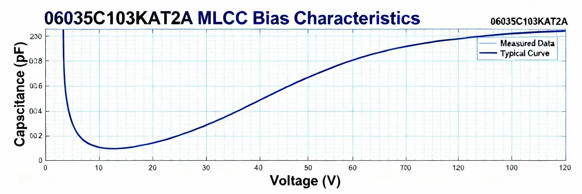
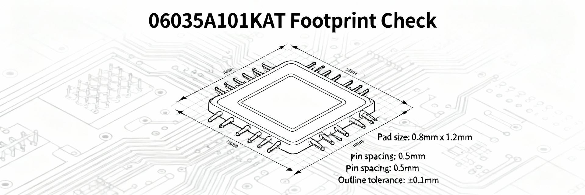
Evidence: Manufacturer datasheets and independent catalogs consistently highlight DC-bias capacitance loss, temperature dependence, and mechanical vulnerabilities as primary concerns for small-package X7R parts. Explanation: This article summarizes benchmark metrics, common failure modes, a repeatable test plan, and actionable QC/procurement checklists so teams can evaluate parts such as 06035C271K4Z2A with repeatable data and clear acceptance criteria. Background: Why choose a 0603 270pF X7R? Key electrical & mechanical specs to watch Point: The 0603 package with nominal 270pF is attractive for space-constrained decoupling and filter roles but carries dielectric-specific trade-offs. Evidence: Typical spec checklists show C_nominal 270 pF, tolerances ±1%–±10%, common voltage ratings 16–50 V, X7R temperature class rated for −55°C to +125°C, and aging behavior noted in vendor literature. Explanation: Designers must monitor aging (ppm/month), DC-bias shift and permitted operating voltage; a short spec table below provides a concise checklist for incoming-inspection review. FieldStandard Specification / Example C_nominal270 pF Tolerance±5% / ±10% Voltage16 V / 25 V / 50 V Temp range−55°C to +125°C Aging rate~0.5–1.5% per decade Typical applications and design constraints Point: 0603 270pF X7R parts are commonly used for bypassing, RF matching elements, and compact filter networks where board area is limited. Evidence: Field reports and bench data indicate DC-bias capacitance loss of 10–35% at 5–10 V and elevated susceptibility to assembly-induced cracks in thin boards. Visualized Risk: Capacitance Loss vs. DC Bias 0V Bias 100% C 5V Bias -18% Loss 10V Bias -35% Loss Explanation: Where capacitance stability under bias is critical (precision timing, narrowband RF), X7R may be unsuitable; the team should select alternative dielectrics or larger packages to meet stability requirements. Lab benchmark summary: electrical performance metrics to report Recommended metrics and how to present them Point: Reporting a standard metric set enables apples-to-apples supplier comparisons for MLCC evaluation. Evidence: Accepted benchmarks include initial capacitance (C0), percent change vs DC bias (0V, 1V, 5V, 10V), C vs temperature across −55°C to +125°C, dissipation factor (DF) or ESR, insulation/leakage current, aging rate, and Q vs frequency. Explanation: Visuals should include C vs DC-bias curves, C vs temperature curves, and histograms of initial C spread; summary tables must report mean ± SD and 95% confidence intervals for transparency. Test setup & sampling notes (repeatable, reproducible) Point: Reproducible results require controlled sampling, calibrated equipment, and documented preconditioning. Evidence: Recommended practice uses calibrated LCR meters at specified test frequencies (e.g., 1 MHz for small caps), controlled temperature chambers, defined solder reflow profiles, and pre-bake for moisture-sensitive parts. Explanation: Specify sample sizes (minimum 30 pcs per lot for basic characterization), report mean ± SD, and retain raw data to compute 95% CIs and enable later forensic review. Reliability & failure-rate analysis: lab stress vs field returns Common failure modes and root causes Point: Several discrete failure modes account for the majority of observed MLCC field issues. Ceramic cracking: From assembly/board flex. Electrode delamination: Manufacturing defect. Capacitance drift: Under DC bias or temperature aging. Insulation breakdown: Increased leakage current. Microfractures: Resulting from thermal cycling. Explanation: Each mode has diagnostic signatures—sudden drop in C indicates cracking, progressive leakage rise signals insulation breakdown—and points to assembly stresses, inadequate derating or poor PCB mechanical design. How to quantify failure rates: FIT, MTBF and confidence bounds Point: Converting accelerated failures into operational rates requires careful modeling and transparent reporting. Evidence: FIT (failures per 10^9 device-hours) and MTBF calculations depend on observed failures, total test hours, and acceleration models such as Arrhenius (temperature) or Coffin–Manson (thermal cycling). Explanation: Report failures per million device-hours with 90% confidence intervals, state acceleration factors and test conditions, and avoid over-extrapolation from tiny sample sizes; recommend stating sample size and censoring rules explicitly. Step-by-step test plan to benchmark 0603 270pF X7R Phase 1: Sample selection, board-level assembly and preconditioning Point: Lot-level sampling and realistic assembly simulation are essential to expose assembly-sensitive failures. Evidence: Use lot sampling rules (e.g., 30–100 pcs per lot), apply representative reflow profiles, and simulate board flex or multiple reflow cycles. Explanation: Retain samples post-test for failure analysis and require suppliers to provide process flow documentation to correlate assembly steps with observed failures. Phase 2: Core electrical and mechanical tests (procedures & criteria) Point: Prioritize tests that reveal DC-bias sensitivity and mechanical robustness. Evidence: Core tests include initial electrical (C/DF/IR), DC-bias sweep, temperature cycling (−55°C↔+125°C), thermal shock, high-temperature biased life, and board flex. Explanation: Suggested pass/fail thresholds: capacitance shift within tolerance ±10% of C0, leakage below specified µA/V threshold, and no cracking visible under X10 inspection. Design & mitigation strategies to lower failure risk Design rules and derating best practices Point: Conservative design rules reduce DC-bias and reliability risk for X7R small packages. Evidence: Practical rules include voltage derating (use higher VR or larger package), select larger case sizes for lower bias sensitivity, and minimize voltage across critical X7R caps. Explanation: Where bias-induced C loss is unacceptable, specify alternate dielectrics or increase capacitance margin; maintain short traces for decoupling to preserve effective ESR/DF performance. Assembly and material choices to reduce mechanical failures Evidence: Effective actions include optimized solder fillet profiles, board stiffening or adhesive underfill for thin PCBs, and selective conformal coating. Explanation: Use a decision flow—accept X7R 0603 when space and margin permit; escalate to 0805 or different dielectric when mechanical or bias risk crosses defined thresholds. Comparative (anonymized) benchmark case study template Point: A standardized table enables rapid supplier triage during qualification. Lot ID N C mean (pF) %Δ @5V Leakage (µA) Failures FIT est Supplier A 50 269 ± 4 −18% 0.01 1 25 Supplier B 50 271 ± 6 −28% 0.05 3 75 How to interpret results and make procurement decisions Explanation: Use threshold-driven outcomes: accept, accept with conditional monitoring, or reject and require corrective action; document decisions and retain failing samples for analysis. Red flags include systematic bias sensitivity >20–30% loss. Action checklist for QC, procurement and field monitoring Incoming inspection & supplier qualification checklist Datasheet dielectric class (X7R) and temp rating verification. Lot-based sample tests (initial C/DF/IR, DC-bias sweep). Supplier process flow and reliability report review. Sample retention policy enforcement. Field monitoring, lifecycle tracking and replacement triggers Evidence: Track KPIs such as observed field failure rate vs expected FIT and board-level symptom logs. Explanation: Maintain automated logs with lot, date code, failure symptom, and board ID to enable trend analysis and timely supplier escalation. Summary MLCC 0603 270pF X7R parts trade compact size for measurable DC-bias and mechanical risk; benchmark metrics must include C vs bias, C vs temperature, DF, leakage, and aging. Standardize tests (sample size, calibrated LCR, thermal chambers, preconditioning) and report mean ± SD with 95% CIs to ensure transparency when comparing lots. Mitigate failures via voltage derating, larger packages where needed, optimized solder/board mechanical design, and a documented incoming-inspection plus field-monitoring program. Use the provided supplier comparison template and follow threshold rules (accept / conditional / reject); include product codes (e.g., 06035C271K4Z2A) in lot records for traceability. Note: For procurement traceability, include the part code 06035C271K4Z2A on inspection forms and retain failing samples for root-cause analysis to close the data loop between QC and field monitoring.

2026-01-29 19:40:06
Top