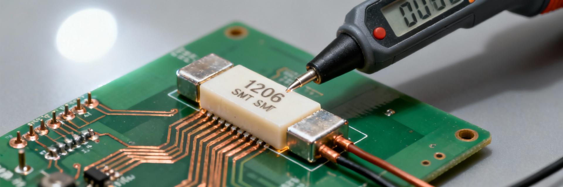
头部 组件族 1206(3216公制) 应用 过电流保护 执行摘要部分 点:本指南将数据手册指标和实验室测试报告转化为工程师评估的简洁参考。0437004.WR部分 证据:该1206系列的供应商文档和分销商测试摘要强调了额定电流、电压等级、跳闸曲线、分断容量和热限制。 解释:工程师在提交设计之前需要一个实用的综合,将这些规范映射到董事会级别的风险和资格步骤。 点:使用此文档来优先处理减少现场故障的测试和集成检查。 证据:分销商笔记中报告的常见故障模式主要集中在回流损坏和曲线外跳变行为。 解释:一个专注的实验室验证计划可以减少昂贵的返工,并确保所选的SMT熔断器满足应用裕量和安全要求。 背景部分 背景:什么0437004.WR级SMT引信和当使用它们 定义和外形尺寸 点: 0437004.WR-class parts are 1206 (3216 metric) fast-acting SMD fuses used for board-level overcurrent protection. EvidenceDatasheets for this family specify low-profile ceramic bodies and thin-film fuse elements optimized for reflow soldering. ExplanationDesigners should treat these as board-mounted sacrificial elements; common PCB constraints include limited board area, tight height envelopes, and required solder fillets for reliable joints.示意说明:使用1206的垫位模板,并遵循推荐的陆地格局公差。 选择前要检查的关键评级 ◈ 额定电流:设置标称负载能力。 ◈ Voltage RatingEnsures dielectric safety limits. ◈ I²t & Trip Curve定义与上游保护的协调。 ◈ 突破能力:确定短路情况下的生存能力。 技术规格组 Technical specsdatasheet breakdown for 0437004.WR Electrical specifications (how to interpret) Parameter Typical Value (1206 Family) Impact on Design 额定电流 ~4 A类 名义作阈值;与跳闸电流不同。 额定电压 32V-63VDC Max circuit voltage to prevent arcing after blow. Breaking Capacity Up to 50A @ Rated Volts Survival limit during catastrophic fault events. Thermal & mechanical specifications 工作温度:-55°C至+125°C 热降额对于升高的环境是必需的。 焊接:回流兼容 Follow peak soldering temp specs to avoid element damage or micro-cracks in ceramic body. Test Data & Methods Test data & test methodsverifying 0437004.WR performance in-lab Standard tests to run Point基本的台架测试包括DC电阻、时间-电流(跳闸曲线)、浪涌/断裂能力、热循环和可焊性/回流烘烤。 证据:实验室程序使用源表、高速电流探头和热室。 解释:DC电阻确认低串联损耗;跳闸测试验证曲线符合性;浪涌测试验证故障能量下的断裂能力。 Common Failure Modes No-Trip/Delayed TripRisk of downstream fire. Nuisance TripsDue to improper I²t margin. 阻力漂移:在激进的回流循环之后。 机械开裂:可见缺口或内部元件损坏。 应用科 Typical applications & troubleshooting case studies Battery Protection Used in regulator input rails and USB power management where rapid interruption is critical. Telecom Signaling Protection for data lines and signal paths where board space is highly constrained. 现场诊断 检查表:测量DCR,检查土地格局方向,并识别上游短路故障。 采购清单 采购和集成清单 购买清单 Confirm exact part-code suffixes. Verify packing format (reel/tape). Request independent test reports. Require lot traceability for production. Qualification Plan 回流鉴定(峰值温度浸泡)。 负载下的功能验证。 裕度测试(110%电流浸泡)。 定义明确的通过/失败标准。 摘要部分 Summary Verify the0437004.WRdatasheet for exact Specs—current, voltage, trip curve, breaking capacity, and thermal limits—before selection. Run a concise qualification setDC resistance, time-current (trip) tests, and surge/breaking-capacity testing; inspect after reflow. 遵循购买和集成清单,确认零件代码、包装,并包括生产前验证计划。 常见问题手风琴部分 常见问题 如何读取时间-电流曲线0437004.WR-style SMT fuse?▼ 点:读取曲线显示给定过流时的保持时间和跳闸包络。 证据:数据表曲线用公差带绘制电流倍数与跳闸时间。 解释:比较测量旅点的曲线;一部分,旅行持续的内部带的标准。 协调、确保上游设备的明确的早期或I2t限制匹配的上游的保护目标。 1206 SMT保险丝需要哪些回流预防措施?▼ 点:遵循保险丝回流温度曲线,并限制在峰值温度下的停留时间。 证据:数据表规定了焊接时的最大峰值温度和超过液相线的持续时间。 解释:过度的热暴露会导致微裂纹或元件改变,从而导致故障;使用推荐的焊盘模式,避免机械弯曲,并进行回流后电气检查。 SMT保险丝生产签字的实际通过/失败标准是什么?▼ 点:定义签署的电气、机械和热标准。 证据:常见的标准包括在数据表公差范围内的行程行为、直流电阻不超过指定阈值,以及经过热循环后无可见损坏。 解释:需要在使用该部件进行生产前,进行一个功能测试的样品卷轴测试,包括按指定要求的功能行程和浪涌生存能力,并记录批次可追溯性。
2026-01-21 13:36:06
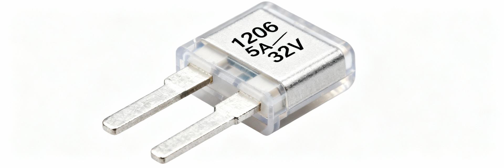
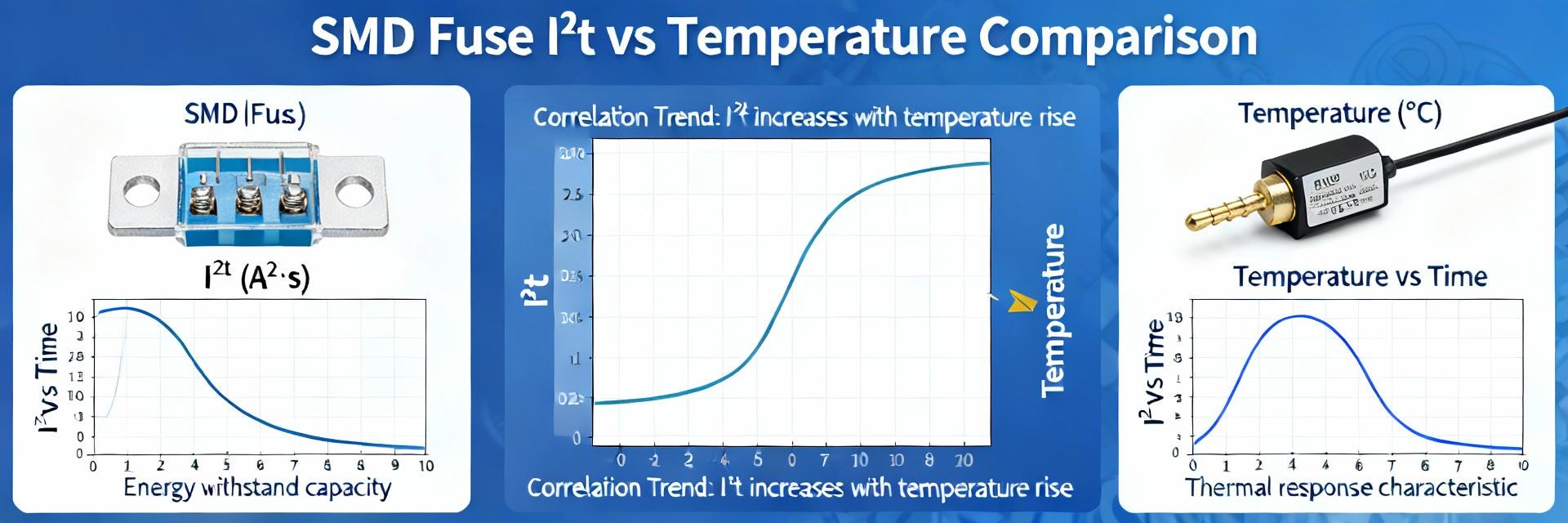
设计逻辑 设计师选择需要空间、可预测的开路时间和低串联电阻的陶瓷/薄膜芯片保险丝。这确保了在高效电源轨上没有显著电压降的情况下提供保护。 图像部分 数据可视化:快速规格 关键额定值一览 参数 典型值 视觉比例 额定电流 5个A 额定电压 32 V(AC/DC) 耐寒性 ~0.016 Ω 标称熔化I²t ~1.936 A²s 注意:在零件选择时,请从正式数据表副本中确认确切数字。 技术规格部分 电气 电气特性 关键条目包括额定电流、额定电压(AC/DC)、耐寒性和时间-电流曲线0.016 Ω限制稳态电压降1.936 A²I²t 决定了如何处理浪涌。将 I²t 与功率转换器的浪涌能量进行比较——如果浪涌超过熔断器的 I²t,就会发生不必要的断开。 环境 环境与机械 典型的薄膜熔断器承受-55℃至+125℃,是危害性物质限制指令/无铅兼容,并容忍260°C峰值回流遵循供应商的着陆模式建议,允许热释放,并观察焊膏孔径,以避免在高电流路径中出现墓碑。 测试数据部分 测量性能和实验室结果 推荐基准测试 通过运行直流电流斜坡并绘制时电流曲线来复现数据表声明。使用电子负载和高速数据采集进行时开测量。建议至少采集10个样本以获得统计置信度。 解释实验室编号 一个名义上的熔化I²t约为1.936 A²s意味着在那种能量下可以承受短时、高浪涌的脉冲。确保断路器额定值(≈50 A)超过你最坏情况下的预期故障电流,以避免危险故障模式。 案例研究 & 布局 应用和集成示例 案例场景:适用于USBPD电源轨、小型设备电池馈电、12 V/24 V子系统和栅极驱动电源。对于大容量电容器或电机等高浪涌负载,请验证I t与浪涌能量或实施软启动电路。 PCB最佳实践将保险丝放置在靠近受保护源的位置。避免在器件正下方布线热过孔,并与热敏元件保持间隙。检查清单:验证焊盘图案尺寸、焊膏孔径和方向。 设计清单 前期制作清单 确认电流和电压是否满足轨道要求。 验证I²t是否满足最坏情况下的系统浪涌。 验证中断能力(50A @ 32V)。 将封装与供应商的1206图纸相匹配。 常见故障和修复 麻烦打开:涌流超过I t→添加软启动。 墓碑:不均匀的焊膏体积 → 调整锡膏模板。 阻力转换:过度的重排热 → 优化配置。 概述部分 摘要 的0437005. WR是一款紧凑、快速动作的5 A/32 V薄膜SMD保险丝,非常适合许多低压PCB保护角色,其中空间和可预测的清除是优先考虑的。 紧凑型保护:1206占地面积,提供适用于USB PD和电池馈电的快速清除。 设计关键I²t标称熔化(~1.936 A²s)决定了浪涌处理能力。 验证基础要素:生产签发前的强制时电流绘图和中断测试。 FAQ手风琴 常见问题 如何0437005. WRI²不影响涌流处理?+ I²t represents the energy required to melt the fuse element; a nominal ~1.936 A²s value means short-duration current spikes below that energy typically won’t open the fuse. Compare measured inrush I²t (integral of I² over time) to the fuse I²t—if system inrush exceeds fuse I²t choose soft-start, NTC/inrush limiter, or a different fuse with higher I²t. What test should I run to verify0437005.WRinterrupt capability?+ 执行中断测试在额定电压与一个潜在的错当前的说明中断的评价(~50)。 使用受控的高流源和高速的捕捉到确保的保险丝清除没有持续电弧;重复跨越几个样本,并在提高的环境,以验证的保证金和安全。 典型的回流曲线会损坏吗0437005. WR在组装过程中?+ Most thin-film 1206 fuses tolerate standard Pb-free reflow (peak ~260 °C for short duration) but tombstoning or elevated resistance can occur with incorrect paste or land patterns. Verify manufacturer reflow limits, run solderability and post-reflow resistance checks, and adjust stencil apertures as needed.
2026-01-21 13:31:32
头部 工程师优先考虑可预测的过流保护;汇总的实验室测试摘要和现场故障调查通常报告故障时间差方差对电路板级可靠性产生重大影响。本文分析了1206贴片保险丝(1.5A,63V), summarizes observed failure data trends, and provides reproducible test methods plus design recommendations for engineers citing lab and field sources where numeric claims are reported. Scope:Focused bench and environmental metrics, common failure modes, statistical analysis approaches, standardized test protocols, and practical derating and mitigation guidance for power-rail and battery-protection applications. The discussion is data-first, intended for design and reliability engineers needing reproducible results. Section 1 Background: Understanding the 1206 SMD Fuse 外形尺寸、电气额定值和通用规格 1206占地面积(公制3.2×1.6毫米)包含可熔元件,尺寸适合空间有限的板级保护。一个典型的额定63V的1.5A保险丝提供延时或快速作用特性;根据结构,耐寒性通常在几十到几百毫欧之间。关键术语包括I²t(融合能量), hold current, blow current, and derating rules versus ambient and surge profiles. Typical Application Domains and Functional Role Common uses include power-rail protection on USB/charger rails, battery pack modules, and downstream board partitions where serviceability is limited. Trade-offs versus larger footprints favor low profile and lower parasitic inductance but reduce peak I²t capability. Section 2 Performance Metrics & Benchmarks 电气性能指标 基本电气测试:测量的保持电流(Ih)、熔断电流(Ib)和时间电流曲线。以下是预期性能范围的可视化分布: CSS数据可视化 保持电流(Ih) 0.6-1.0×额定 Blow Current (Ib) 1.6 – 3.0 × Rated Cold Resistance 10 – 200 mΩ Metric 典型范围 验收阈值 保持电流(Ih) 0.6-1.0×额定 25°C无跳闸 Blow Current (Ib) 1.6–3.0 × rated Open within defined curve Cold Resistance 10–200 mΩ ±15%批次差异 环境与机械指标 测试并记录回流耐受性、热循环(40°C至高温环境)和电路板挠性。A验收标准通常依赖于电漂移(例如,应力后电阻变化 第三条 失效数据:模式和统计模式 Common Failure Modes ● Clean Fusing:Normal open-circuit from overcurrent. ● 潜在打开:后回流或热机械断裂。 ● 参数漂移:阻力逐渐增加。 ● CTE Mismatch:Solder-joint failure due to thermal expansion. Statistical Analysis Present failure data with sample sizes每手≥30.利用方法威布尔分析提取形状和比例参数。可视化可观的累积失效图和箱形图,以揭示批次漂移和异常值。 第4 Recommended Test Methodology Lab Setup & Protocols Use synchronized current and voltage capture at≥100 kHz sampling. Perform controlled slow ramps to determine Ib and pulse surge profiles (10 ms, 100 ms, 1 s) to capture I²t behavior accurately. 报告模板 文件:第ID部分、批次、电路板占地面积、环境温度、测量Ih/Ib、打开时间和测试后电阻。这些数据对于风险评估和生产验证至关重要。 第5节 设计与可靠性建议 选择和降额 目标连续电流≤ 70–80%名义上的 验证超过63V的浪涌电压额定裕度。 匹配时间滞后与快速响应以加载浪涌。 缓解和生命周期 在PCB布局中提供热释放。 避免在保险丝附近使用尖锐的板弯曲线。 定义现场监测的检查间隔。 总结 摘要 ✓1206 SMD保险丝用于保护空间受限的低电压线路;在选择前需验证Ih/Ib和I²t是否符合预期的浪涌曲线。 ✓失效数据应收集 ≥30 个样本,以高采样率记录时电流曲线,并使用威布尔方法进行分析。 ✓降低连续电流至≤80%,将特性与涌流相匹配,并实施电路板/布局缓解措施以获得生命周期反馈。 常见问题解答部分 常见问题 我应该使用什么测试电流来表征1206 SMD保险丝?+ 在多个点进行表征:在0.8–1.25倍额定值下进行稳态保持验证,缓慢斜坡以找到爆破阈值,以及脉冲浪涌(例如,10 ms、100 ms、1 s)以捕获I²t行为。记录打开时间,并在脉冲测试中使用≥100 kHz采样率计算I²t以确保准确性。 工程师应该如何报告和解读主板认证的失效数据?+ 报告标准字段:部件ID、批次、PCB封装、环境、Ih、Ib、开启时间、测试后电阻和视觉备注。将失效时间拟合到威布尔分布,报告比例和形状因子及其置信区间,并将失效与I²t和环境应力相关联。 哪些降额和布局检查可以防止1.5A保险丝的干扰断路?+ 在升高的环境下,将连续电流降为额定电流的70-80%,确保浪涌I t容量超过预期的瞬态能量,验证回流兼容性,并保持与热源的热隔离。为63V提供足够的爬电/间隙,避免机械应力集中。
2026-01-21 13:27:08
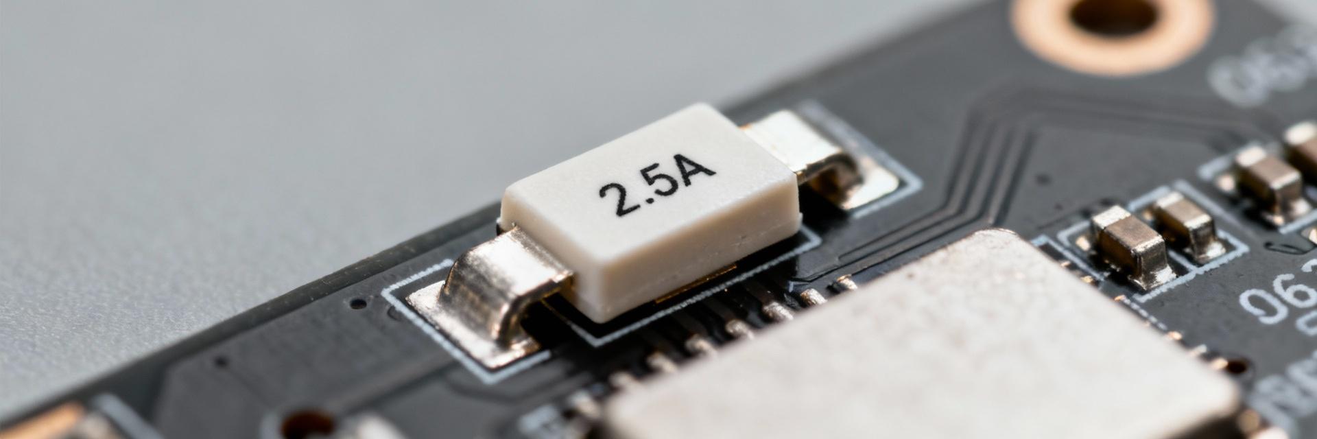
SEO优化标题 设计人员在选择微型SMD保险丝时经常面临令人讨厌的打开、认证失败或电路板损坏。这043802.5WRA是一款紧凑型0603解决方案,可满足空间受限的电源保护需求。本指南解释了如何选择和使用具有清晰检查的2.5A保险丝——电气匹配、PCB/装配兼容性和验证测试——因此团队可以避免常见陷阱并获得可靠的现场性能。 背景部分 Background: What the 043802.5WRA 0603 SMD Fuse Is and Where It Fits Point:The043802.5WRAis a fast-acting 0603 surface-mount fuse rated nominally at 2.5A for low-voltage DC and specified AC ranges. 证据:数据表条目列出额定电流、电压、中断容量、机壳尺寸(0603 / 1608指标)及典型冷阻。 解释:这些规格定义了零件的适用范围——小型便携式电子设备、模块输入导轨以及紧凑型电信或汽车子组件,其中自动化放置和最小的电路板空间是优先考虑的。 电气规格表和可视化 Key Electrical and Physical Specs to Know Critical specs determine suitability. Typical values include rated current 2.5A and voltage rating up to common low-voltage system levels. Spec Typical Value Why it Matters 额定电流 2.5A 定义允许的连续负载 套餐 0603(1608公制) Space & placement constraints Blow Type Fast-acting Protects sensitive parts; may nuisance-open Interrupt Rating 有限 必须超过可用故障能量 典型应用和设计背景 0603保险丝在空间和自动化装配方面表现出色。常见用途包括紧凑型传感器板上的输入导轨、电信模块和小型PCB上的分布式电源。当优先考虑PCB面积和低热质量时,请选择0603。 性能部分 Data & Performance: Interpreting Selection Specs Time-Current Curves Read curves to ensure expected surges (inrush) do not cause nuisance opens. Rule-of-thumb: continuous current should generally be ≤ 70–85% of rated current depending on thermal conditions. PCB & Assembly Use vendor ECAD footprints and follow reflow limits. For automotive/industrial use, ensure vibration and thermal cycling qualifications are met to avoid internal damage. 选拔指南 如何选择正确的043802.5WRA 满足电气需求 应用简单的公式:额定电流≥连续负载/降额系数. Confirm blow time at surge current is greater than expected inrush duration. Add soft-starts if inrush is long. Constraints & Trade-offs Smaller packages reduce interrupt capability. Use a decision matrix to balance board space, fault energy, and sensitivity of protected circuitry before finalizing the 0603 form factor. Installation Best Practices How to Install & Use on PCB: Best Practices 安装方式:验证足迹与制造商ECAD匹配,以防止墓碑。 焊接:严格遵守回流温度/时间限制;过多的热量会对保险丝元件造成压力。 测试:实现基准电流斜坡测试和热循环,以揭示边缘设计。 实际应用案例 实际应用案例与常见故障模式 成功场景 小型传感器模块和多轨PCB在故障能量适中且空间有限的情况下,受益于0603保护。 故障预防 通过修改散热布局和验证组件回流焊曲线,防止出现有害开路。 清单与收获 快速预购清单 ✔确认系统电压与数据手册是否一致。 ✔请求 ECAD/3D 文件。 ✔订购用于 I²t 测试的样品。 关键摘要 •2.5A 快速起作用 0603 设计。 •非常适合空间有限的DC轨道。 •仔细匹配浪涌/降额。 常见问题手风琴 常见问题 这是什么 2.5A 保险丝的额定行为?+ 答:保险丝的额定电流为2.5A,具有快速熔断特性;请查阅数据表时间-电流曲线,了解其承受额定电流倍数的时间,并确保可用故障能量在其中断额定值内。 如何在工作台上测试2.5A SMD保险丝?+ 使用可编程电源进行受控电流斜坡测试,监测设定电流倍数下的开启时间,并在样品上重复。记录电流并与预期故障能量进行比较;在引发故障时始终遵循安全实验室程序。 是什么导致小型SMD熔断器产生干扰性开启?+ 答案:常见原因包括环境/PCB加热的降额不足、持续时间超过吹扫时间的浪涌电流、过度回流热暴露导致的组装损坏,或实际故障能量下的中断能力不足。 动画视觉效果(通过关键帧实现极简风格)
2026-01-21 13:22:15
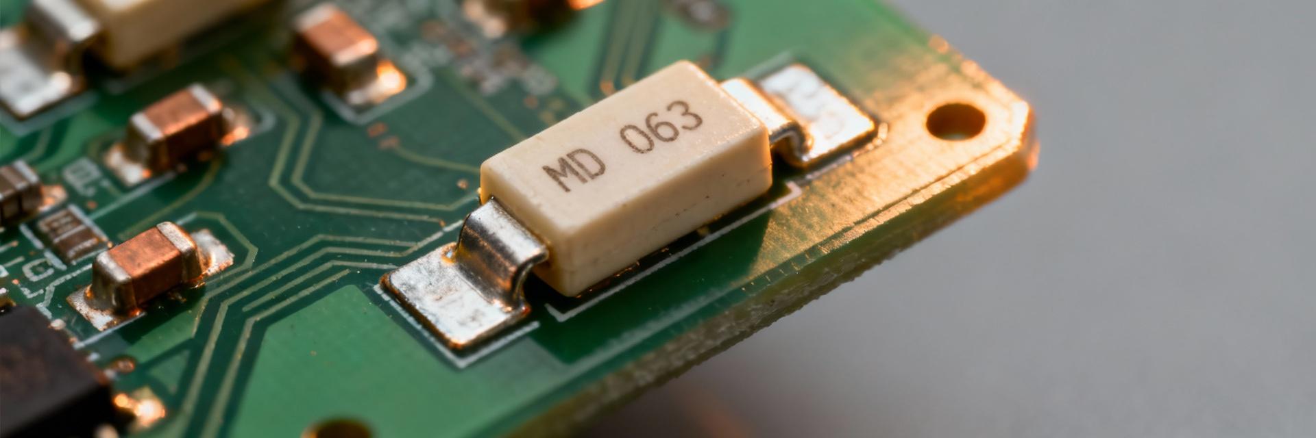
标题部分 对现代物联网和便携式电子产品的高密度保护的全面技术洞察。 介绍卡 现代便携式和物联网设计正在将更高的电流密度推向越来越小的PCB,将设计师推向紧凑型保护设备。行业抽样显示,更多的电路板将多功能保险丝和快速作用的芯片保险丝放置在小于2毫米的占地面积上;这SMD fuse 0603是设计师需要 ~1–2 A 保护同时保留空间时的常见选择。 本指南重点介绍了额定1.75A的设备在电气方面的表现,以及如何实现可靠的PCB焊盘和布局,弥合数据手册规格与实际装配之间的差距。 为什么 0603 节段 为什么 SMD 熔断器 0603 在紧凑型电源保护中很常见 典型用例和系统级权衡 典型的产品包括可穿戴设备、紧凑型传感器和小型电源轨模块。这些系统共享紧张的面积预算,通常需要个位数的安培保护。选择1.75A的保险丝可以交换热质量和中断鲁棒性以换取占地面积;更大的保险丝主体提供更高的中断能量和热惯性,而可重置的替代品可以减少一次性更换,但会增加电阻和尺寸。 包装解剖学(1.6×0.8 mm) 0603 的机型限制了热裕度和机械余裕。1.6 × 0.8毫米陶瓷或环氧树脂机体,端盖镀层,内部元件薄,热容量小且国际单位数有限。端盖冶金和终端方式会影响焊锡的润湿和机械稳健性;狭小的间隙需要精心设计焊盘,以确保热量得到管理,并在回流时正确形成。 数据分析和视觉 电气性能指标 可视化Fuse行为 额定电流(1.75A)- 持续运行 融合当前(典型为额定值的200-250%)- 瞬时熔化 *热能容量与故障能量的表示* 关键规格:额定电流 & I²t 当存在浪涌或瞬态时,读取曲线是必要的。时间-电流图表明,可以容忍短浪涌而不会出现干扰。选择一个时间-电流曲线可以清除真正故障但仍然存在浪涌的设备;当您的电路有电机、电容组或电池连接浪涌时,使用I t比较瞬态能量容忍度和尺寸裕度。 抵抗力降低 串联电阻控制跌落和热量。芯片保险丝的DC电阻很小,但可以测量;更高的电阻会增加1.75A的功率损耗(P=I R)。为您的导轨指定最大额定电压,从数据表中应用温度降额以获得升高的电路板温度,并确认中断额定值-DC中断性能通常低于AC。 可靠性表 可靠性和测试条件 因子 实际影响 缓解策略 安装 & 重新流化 侵略性的无铅回流可能导致微裂纹。 按照制造商的概况;确保即使垫湿润。 衰老影响 阻漂移过长期的热循环。 验证高温环境中的长期稳定性。 PCB铜 起散热作用,改变跳闸温度。 使用热过孔来标准化散热。 方法指南:足迹 设计 PCB 封装(0603) 从物理体导出垫片,并留有圆角余量。步骤:基于组件长度/宽度(1.6 × 0.8 毫米),每端允许约 0.2–0.4 毫米的圆角重叠,并保持中心间隙与端接间距匹配。 保守的足迹,(mm)衬垫长度:0.9–1.0垫宽度:0.8–1.0差距:0.2 – 0.4 紧空间的占用(mm)垫片长度:0.6 – 0.8填充宽度:0.6 – 0.8差距:0.3 – 0.4 Stencil Tip: Reduce paste apertures 10–20% per pad for reliable solder volume and to prevent bridging. 安装 & 散热 布局与布局考虑 热降额和倒铜 保持至少0.5-1.0毫米的距离远离大型铜区域或包括散热装置;对于敏感网络,使用窄热辐条隔离保险丝垫,使其热时间常数与保险丝额定值对齐。这种调整有助于在长时间过载期间进行可预测的操作。 迹线宽度和通孔 对于持续的1.75A,使用短而宽的迹线;对于1盎司铜,根据允许的温升,目标宽度为1.5-3.0毫米。将保险丝放在电源附近,最小化负载的迹线长度,并在电流必须在层之间传输以减少电阻加热的地方添加缝线。 清单与验证 采样前的选择清单 ✔验证额定电流和时间电流曲线是否与冲击电流匹配。 ✔确认DC电阻和1.75 A的预期压降。 ✔检查DC系统的中断额定值和最大额定电压。 ✔确认工作温度窗口和包装公差。 ✔Record preferred part code (e.g.,04381.75WR) for BOM. Validation & test plan for prototypes 后回流的视觉和显微镜检查的鱼片。 连续性和耐核查与数据表。 受控过电流浸泡测试和热成像。 机械冲击和三循环热循环。 记录结果,必要时反复修改垫子或模板。 Summary Summary For compact power protection where space wins, the SMD fuse 0603 offers a practical balance for ~1–2 A rails when designers account for limited thermal mass, DC resistance, and interrupt capability. Key checks are time‑current behavior, I²t for transients, pad design for reliable fillets, and layout choices that control heat and parasitics. Prototype validation—reflow check, current soak, and imaging—should precede production to ensure consistent field performance. Use the 1.6 × 0.8 mm package data as the starting point for pad derivation. Evaluate time‑current curves and I²t to tolerate inrush while still clearing real faults. 保持保险丝靠近电源,并隔离大的铜浇注。 常见问题手风琴 常见问题 与较大的保险丝相比,1.75A保险丝在PCB上的表现如何?+ Smaller chip fuses heat up and clear faster due to lower thermal mass; they offer quick interruption for small faults but have lower I²t and interrupt energy than larger fuses. On PCB, ensure pad and copper layout neither dissipate excessive heat nor prevent expected trip behavior. What PCB footprint practices ensure reliable operation for a 0603 fuse?+ Design pads with controlled overlap and a gap matching termination spacing, reduce paste apertures 10–20%, use a 0.12 mm stencil, and verify fillet formation post‑reflow. Keep pads away from large copper or add thermal spokes to tune dissipation. Can I use a resettable alternative instead of a 1.75A fuse?+ 可复位的PTC以较低的跳闸精度和更高的电阻换取自动复位能力;它们适用于重复的浪涌环境,但会增加电压降,并且可能无法清晰地清除高能故障。在更换之前验证热和电压影响。
2026-01-21 13:17:38
Detailed analysis of I²t shifts and thermal derating across -55°C to +150°C for high-reliability PCB power rail protection. Lab measurements and published time–current curves indicate that I²t and open time for the 0441005.WR can shift substantially across a typical −55°C to +150°C operating window—a critical concern for PCBs with high inrush or elevated ambient conditions. This report compares measured I²t behavior, quantifies temperature impacts, and provides practical test and design guidance for engineers specifying this SMD fuse. The purpose is threefold: 1. Explain I²t measurement and interpretation. 2. Demonstrate how ambient and board thermal coupling alter hold/clear behavior. 3. Present reproducible lab methods and design mitigations for US engineering teams. Background: 0441005.WR SMD Fuse — Specs & Application Context A compact, fast‑acting chip fuse rated for short‑circuit protection is commonly specified with the following nominal characteristics. Selection criteria must balance fault clearing energy versus allowed let‑through for downstream components. Key Specifications at a Glance Parameter Nominal Value (Datasheet Field) Package 0603 (Chip Fuse) Rated Current 5 A Rated Voltage 32 V Speed Class Fast‑acting Operating Temperature −55°C to +150°C Rated I²t Verify melt vs. arcing values Actionable Note: Confirm whether the datasheet provides separate melt‑I²t and arcing‑I²t values; if only one is given, flag that gap and request manufacturer test data or measure in‑house. Typical Use Cases & Design Constraints Constraint 1: Maximum expected inrush energy (I²t) must remain below fuse melt I²t with safety margin. Constraint 2: Continuous ambient/board temperature can reduce allowable let‑through energy — derating required. Constraint 3: PCB thermal mass and nearby heat sources dictate effective fuse temperature and behavior. I²t Performance: Definition, Test Data Interpretation & Expected Curves I²t Explained & Measured I²t is the integral of I² over time (∫I² dt), representing let‑through thermal energy during clearing. Differentiate melting I²t (energy to melt the element) from arcing I²t (energy during sustained arc) when both values are reported. Capture: ≥100 kS/s waveform sample rate. Units: A²·s. Interpreting Measured Curves Measured curves often deviate from datasheet graphs. Acceptable deviations depend on test fixture resistance, sample variability, and measurement method. Rule‑of‑thumb: Require 20–30% margin between inrush I²t and melt I²t. Temperature Limits & Thermal Derating The stated operating range (-55°C to +150°C) describes survival, not guaranteed clearing consistency. Designers must consider local thermal rise on the PCB. Conceptual I²t Derating vs. Temperature 25°C 100% 85°C 85% 125°C 70% 150°C 55% *Interpolated data based on standard 0603 fast-acting fuse characteristics. Test Methodology: Lab Setup for 0441005.WR Required Equipment Programmable current source (fast slew rate). High-speed oscilloscope (100 kS/s minimum). Calibrated thermal chamber or hot plate. Low-inductance test leads and copper solder pads. Procedure Best Practices Run baseline room-temp tests at multiple multiples of current. Measure at -40°C, 25°C, 85°C, and 125°C. Use ≥10 samples per condition for statistical mean/std dev. Design Recommendations & Failure‑Mode Mitigations Selection Checklist ✓ Confirm worst‑case inrush I²t ✓ Apply 20-30% Safety Margin ✓ Evaluate PCB Thermal Environment If inrush exceeds margins, consider: NTC inrush limiters, slow-start circuits, or higher-I²t fuses. Avoid placing power-dissipating components immediately adjacent to the fuse. Summary I²t and temperature limits materially influence the suitability of the 0441005.WR for inrush‑heavy and high‑ambient designs. Engineers should extract datasheet melt/arcing fields, run controlled I²t vs. temperature sweeps, and apply a conservative 20–30% margin. The provided test methodology enables reproducible qualification and practical mitigations to reduce nuisance opens while maintaining protection. Key Summary Points: Design margin ≥20–30% between inrush I²t and melt I²t. PCB thermal rise shortens time‑to‑open and reduces allowable I²t. Record raw waveforms at ≥100 kS/s for precise calculation. Mitigate via thermal layout, soft‑start, or NTC limiters. Common Questions & Answers How does 0441005.WR change I²t with temperature? + Measured behavior shows a reduction in allowable let‑through energy as fuse temperature rises: time‑to‑open shortens and melt I²t decreases. Quantify this with temperature sweep tests in 10°C steps and report normalized I²t so designers can derate continuous current appropriately. Can 0441005.WR be used for USB power inrush protection? + The part can be used for USB power lines if measured inrush I²t (including hot‑plug events) remains below the fuse melt I²t with sufficient margin. If not, add soft‑start or an NTC inrush limiter to protect against nuisance opens while preserving short‑circuit protection. What test sample size and statistics are recommended for characterization? + Use at least 10 samples per test condition and report mean and standard deviation for time‑to‑open and I²t. Include raw traces, computed I²t values, and a histogram of open times to show dispersion and support conservative design margins.
2026-01-21 13:11:15
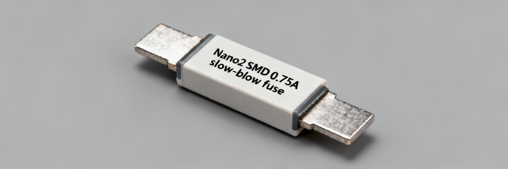
头部 调整过电流保护的工程师通常会查阅保险丝和浪涌保护组件的聚合曲库和实验室数据集来设置安全裕度。本文分析了0443.750DR数据表并提取关键的电气规格,以便设计人员可以放心地将额定电流、电压、中断能力和热限制映射到系统级要求中。 Section 1: Background What is the 0443.750DR? (Background) Point:The0443.750DR是一种表面贴装延时(慢熔断)保险丝,旨在保护电路免受持续过电流的影响。 证据:数据表将其分类为Nano2/443家族带有SMD矩形封装和两个用于回流安装的末端端子。 Explanation:That package and time‑lag characteristic favors inrush‑tolerant protection on board‑level AC and DC rails where repeatability and compact footprint matter. Intended function and typical package Point:Functionally the part interrupts overcurrent while tolerating short surges.证据:该数据表显示,Nano2 SMD外壳的额定额定电压为0.75 A,工作电压等级为250 VAC,具有推荐的接地模式足迹。解释:设计人员应调整零件的方向,以最小化与热源的热耦合,并遵循推荐的占地面积,以在回流和系统内热条件下保持额定性能。 关键用例和系统级角色 点:典型的应用包括板级市电输入、电源和I/O保护。证据:由于存在时间延迟,它在处理电机或大电容负载的浪涌电流时,会吹灭持续故障。解释:系统的参数,确定适用的是线电压,预期的稳定状态和暂时流,允许一系列的阻力和加容,并且需要中断评价安全遵守情况。 第2部分:数据深度挖掘 完整的电气规格(数据深入挖掘) 要点:本节整理了来自0443.750DR数据表,以便工程师可以与系统约束条件进行比较。证据:关键字段包括额定电流、额定电压、 Interrupting Rating、工作/存储温度和时间-电流特性。解释:将这些值提取到采购和验证表中,以便测试和设计团队共享单一事实来源。 绝对最大额定值和工作限制 参数 测试条件 值 额定电流 连续的 0.75 A 额定电压 交流或直流 250 V AC 中断评级 在额定电压下 35 A (典型) 工作/存储温度 -55°C至+125°C 范围 时滞特性 以T-I曲线定义 缓慢的打击 可视化数据表示 当前处理可视化 0A 0.75A (额定) 3.0A(故障区) 需要记录的关键性能参数 要点:超过绝对额定值,记录保持/熔断电流、I2t、电压降和环境降额。证据:数据表提供了时间-电流曲线(保持与时间)和额定电流下的最大电压降。说明:必须记录典型值与保证值;例如,测量的冷保持电流应与保证的最小值相匹配,以避免生产中的干扰性开路。 第3节:数据分析 击穿电压特性和保护特性(数据分析) 要点:对于保险丝,术语击穿电压不是主要指标;相反,介电强度和额定电压决定绝缘性能。证据:0443.750DR指定额定电压和绝缘或爬电限制,而不是Vbr数值。解释:当引入时,这里使用次级关键词击穿电压来对比TVS式器件与保险丝——保险丝是中断电流而不是钳位电压。 解读击穿电压规格和公差 要点:工程师必须将数据表的额定电压和介电测试解释为功能“耐受”极限。证据:数据表将列出额定电压和任何介电耐受或绝缘电阻测试。解释:这些值决定了最大连续系统电压和行间距;它们不像半导体避雷器那样代表开关或钳位阈值。 钳位、能量处理和重复浪涌响应 要点:不适用箝位电压;熔断器的能量处理用I2 t和功耗表示。证据:数据表提供的I2 t和时间电流曲线表明在给定电流下熔断所需的能量。解释:低于熔断阈值的重复浪涌是可以容忍的,但重复的接近熔断脉冲会使元件老化并改变时间电流行为;对预期浪涌曲线应用降额。 第4节:测试指南 如何测试、验证和测量电气规格(方法/指南) 要点:验证需要时序测试、电压降测量和介电性能检查。证据:标准测试设置要求校准的电流源、高精度电压表、温控夹具和T-I曲线测试夹具。解释:控制环境温度,使用四线电压测量法跨接熔断器,并遵循数据手册的测试波形和调节建议,以确保可重复的结果。 推荐测试设置和测试条件 使用步进电流和脉冲电流程序来验证保持和吹扫行为。使用可编程电流源、示波器来捕获打开时间,以及温度室。最小化引线电感并记录电缆布线。 示例测量清单 冷藏电流(在±10%以内) 额定电流压降 T-I曲线一致性检查 吹后绝缘电阻 第5节:案例研究 应用示例和选择场景(案例研究) 1低压串行数据线保护 点:对于预期稳态电流为0.2 A、短路浪涌电流为1.0 A的5 V逻辑电源轨,应选择一个冷保持电流超过稳态电流且在持续故障时熔断的保险丝。证据:0.75 A额定值和慢熔断曲线意味着该器件可以承受短时浪涌,但在长时间1。5–2倍故障。解释:如果信号完整性敏感,可以加入一个小串联电阻或铁氧体;记录示意图和物料清单条目以便审查。 2示例:具有降额功能的电源线浪涌保护 点:对于 120 VAC 输入、环境温度 60°C 和频繁瞬态的情况,应降低连续电流并考虑热叠加效应。证据:该数据表的环境校正系数和时间电流曲线表明,在高温下应按指定百分比降低允许的连续电流。解释:通过模拟最坏情况下的浪涌能量并应用安全裕度(例如充足,≤连续运行额定电流的80%)。 第6节:可操作指南 设计清单:安全限值、降额和安装提示 快速安全和降额清单 工作电流≤额定电流的80%。 Verify Interrupting Rating > Fault Current. Follow exact recommended PCB footprint. Minimize thermal coupling to MOSFETs/Inductors. Account for altitude/pressure if applicable. Troubleshooting Common Issues 常见症状包括烦人的开路、上升的电压降或热退化。补救措施:修改零件选择、改进冷却、增加串联电阻或改用具有更高中断额定值的零件。 关键摘要 关键摘要 The0443.750DRis a 0.75 A Nano2 time‑lag SMD fuse; verify rated voltage and interrupting rating against system prospective fault current and board thermal profile. Critical electrical specs to record are rated current, rated voltage, interrupting rating, time‑current (I‑t) curve, voltage drop, and ambient derating factors for reliable selection. Testing should include cold‑hold, blow‑time at multiple currents, voltage‑drop measurement, and dielectric checks; document pass/fail bands and retain raw captures for review. 最终回顾 回顾:使用该0443.750DR数据表是提取额定电流、电压、中断能力和I-t曲线;通过测量清单验证电气规格,并应用保守降额在最终确定设计之前。 FAQ Accordion Section Frequently Asked Questions How do I verify the0443.750DRrated current in production?+ 使用校准的电流源测量冷保持电流,并监控在指定过电流下打开的时间。将测量的保持时间和打击时间与多个样品的数据表T-I曲线进行比较,以确保批次一致性;维护每批的可追溯记录和示波器捕获。 我应该申请什么样的降额0443.750DR对于升高的环境?+ Follow the datasheet’s ambient correction guidance; as a practical rule reduce continuous allowed current to about 70–80% of rated at high ambient and account for PCB heat sources. Re‑validate time‑current behavior at the elevated temperature to confirm acceptable margins. Can I use0443.750DRfor surge‑prone mains inputs?+ 如果中断额定值和时间电流特性符合预期故障和浪涌曲线,则为“是”。确保器件的中断额定值超过预期故障电流,并应用热和浪涌降额;如果预期能量超过器件的I2 t能力,则选择更高额定值的器件。
2026-01-21 13:04:35
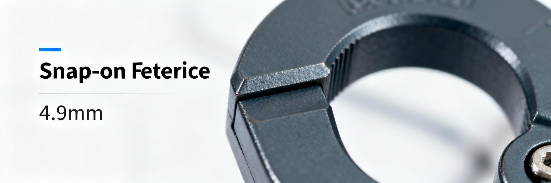
Technical Reference EMI Suppression Bench Sweeps & Datasheet Summaries Measured impedance peaks near 150 Ω @100 MHz with useful attenuation from ~25 MHz to 300 MHz; fits round cables from ~2.5 mm to ~25.4 mm. Point: This article is a data-first technical reference. Evidence: Bench sweeps report a ~150 Ω impedance point and a practical attenuation band beginning near 25 MHz. Explanation: That combination positions the part as a mid‑frequency retrofit suppression element for both data and power lines. Purpose: Decode the part number, summarize physical and electrical specs, outline test procedures, and provide a procurement checklist. Evidence: Covers mechanical dimensions, impedance behavior, installation, and application scenarios. Explanation: Validates fit and predicts performance to reduce risk before production buys. At-a-Glance: Split Core Ferrite Clamp (Background introduction) Quick Spec Snapshot Point: Concise spec snapshot for fast evaluation. Evidence: Inner diameter ~4.9 mm (0.193"), outer envelope ~12–15 mm, body length ~15 mm, weight ≈1–2 g, cable aperture range ~2.5 mm–25.4 mm, rated impedance ~150 Ω @100 MHz. Explanation: Use as a checklist for mechanical fit and mid-band suppression; snap-on retrofit capability. Target Audience Point: Target audience and selection triggers. Evidence: Aimed at design engineers, test technicians, and procurement specialists. Explanation: Ideal for designs with emissions in the 25–300 MHz range requiring non-invasive installation. Performance Visualization: Attenuation Spectrum Useful Band: 25 MHz - 300 MHz 10 MHz 25 MHz (Start) 100 MHz (Peak: 150 Ω) 300 MHz (End) 1 GHz Physical & Electrical Specifications (Data analysis) Mechanical Dimensions and Cable Compatibility Point: Mechanical fit drives selection. Evidence: Inner diameter near 4.9 mm, suitable for single-conductor and small multi-conductor cables. Explanation: Verify cable jackets and connector clearance; use multiple turns if the bundle is smaller than the aperture to maintain impedance. Electrical Characteristics: Impedance vs. Frequency Frequency Point Nominal Impedance Application Priority 25 MHz Rising Attenuation Low-Mid Frequency 100 MHz ~150 Ω Peak Suppression 300 MHz Roll-off Point High Frequency Edge Point: Interpret the impedance spec for attenuation planning. Evidence: Nominal 150 Ω indicates usable common‑mode suppression. Explanation: Select based on whether low‑frequency (below 30 MHz) or high‑frequency (above 300 MHz) suppression is prioritized. Performance, Testing & Interpretation (Data analysis) Attenuation & Insertion Loss Point: Translate impedance curves into practical attenuation. Evidence: S21 sweeps show single clamp provides several dB of common‑mode attenuation; multiple turns add insertion loss additively. Explanation: Use a network analyzer sweep from 10 MHz–1 GHz to compare single vs. multiple passes. Thermal & Mechanical Limits Point: Mechanical and magnetic limits affect long-term performance. Evidence: Can lose effectiveness under DC bias or repeated stress; hinges can crack. Explanation: Include thermal soak and current‑bias tests; inspect clamp retention after torque cycling. Installation & Best Practices (Method guide) Step-by-Step Snap-on Installation 01 Inspect cable for jacket integrity. 02 Position 1–2 cm from the noise source or connector body. 03 Close until latched and verify mechanical retention. Point: Correct placement maximizes suppression. Evidence: Recommended steps are effective for retrofit installs. Explanation: Placing too close to connectors can reduce effectiveness; multiple clamps deliver best results. Strategies for Maximizing Suppression Point: Combine mechanical and routing strategies. Evidence: Routing cables away from noisy circuits and pairing with common‑mode chokes. Explanation: Functional tests and emission scans will confirm gains before production. Applications & Compatibility (Case study) Scenarios USB/Ethernet leads, DC power feeds, and harness entry points. Expect modest single-clamp attenuation (few dB) and larger gains with combined tactics. Interoperability Thick overmolds and braided shields increase diameter. Measure jacket OD under production conditions; consider larger apertures if fit is too tight. Procurement & Selection Checklist (Action guide) Validation Checklist Confirm ID/OD against cable specs. Verify impedance at target frequency. Check RoHS/Flammability standards. Request raw frequency-vs-impedance curves. Logistics & Storage Order samples first. Inspect for cracks or poor latch action on receipt. Store in dry, temperature-stable locations. Mark BOM entries with physical descriptors. Summary Recap: The 0444173951 split-core ferrite clamp is a snap-on solution optimized for mid‑frequency EMI suppression (nominally ~150 Ω @100 MHz). It fits a broad range of small cables and is suitable for retrofit and assembly‑level suppression. ✔ Verify mechanical fit and mid-band suppression (ID ~4.9 mm, 150 Ω @100 MHz). ✔ Inspect hinge retention and seating during sample evaluation to avoid mechanical failure. ✔ Combine multiple clamps and routing for broader suppression; expect additive dB gains. ✔ Prioritize physical fit and measured impedance curves over nominal part numbers. Frequently Asked Questions How should I test a split core ferrite for effectiveness? + Point: A reproducible test confirms expected suppression. Evidence: Use a vector network analyzer to measure S21 insertion loss from 10 MHz–1 GHz with a calibrated fixture. Explanation: This method shows frequency bands where the clamp contributes most and whether additional measures are needed. Can a ferrite clamp handle high DC currents? + Point: DC bias reduces effectiveness for many ferrite materials. Evidence: Common ferrite clamps have modest power handling; permeability can drop under DC bias. Explanation: For applications with substantial DC current, test under representative bias or select materials specified for higher DC tolerance. What are quick checks on receipt to avoid bad lots? + Point: Simple visual and mechanical inspections catch common defects. Evidence: Inspect for visible cracks, chipped ferrite, and hinge action. Explanation: Rejecting damaged samples early prevents field issues and avoids wasted qualification time.
2026-01-21 12:57:35
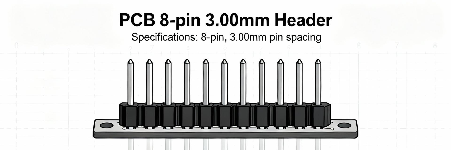
标题部分 这种8位、3.00毫米间距的垂直PCB接头通常为每个电路指定高达5 A,绝缘考虑因素可能达到几百伏-在布局或更换之前必须验证的关键电气和机械值。本摘要从制造商数据表中提取引脚图、机械图纸、电气规格、热限制和测试提示,以支持设计决策。 第1部分:产品概述 产品概述和关键标识符(背景介绍) 零件族和通用描述 点:该组件是一个单排、8位垂直PCB插头,间距为3.00毫米,用于板对板或电缆插头。 证据:外形尺寸适用于控制PCB上的混合信号和适度功率分配。 解释:设计师通常选择这种接头,因为需要紧凑的垂直连接和可靠的焊点,但不需要完全包覆。 部件号解密 要点部件号编码配置、电镀和封装;这些影响电气和机械性能。 证据:典型字段包括系列、位置数量、电镀工艺和包装形式。 解释:验证完成(锡与选择性镀层),配置代码,以及制造商数据表上的任何选项后缀,以确保与焊接和环境要求兼容。 Section 2Mechanical Specs 机械规格与引脚排列(数据分析) 机械图纸定义焊盘布局、引脚编号和锚定特征-根据0436500815在生成足迹之前,请先查看数据表。典型图纸显示了精确的引线间距、极化钉位置和推荐的孔尺寸。即使是0.1毫米的不匹配也会导致焊接缺陷或机械干扰。 引脚表和PCB占用空间指南 引脚 函数 电镀 推荐孔径Ø 1 信号 / 电源 锡 1.20毫米 2 信号 / 功率 锡 1.20 mm ... ... ... ... 8. 信号 / 功率 锡 1.20毫米 第三部分:电气规格 电气规格与性能限制 数值数据可视化 额定电流 5 A 阻力 介电 600 V 额定电流、电压和接触电阻 额定电流和电压决定安全操作范围;设计人员必须确认应用降额的电气规格。在定义的温升下,典型额定值为每个触点5 A;绝缘/工作电压值显示在数据表上。 介电、绝缘和信号完整性 介电强度和绝缘电阻影响安全性和性能。对于混合高压和高速信号,增加额外间隙,考虑屏蔽,并且仅在用于低频信号以上时才检查串扰/阻抗。 第四章:热与可靠性 热学、环境及可靠性等级 运行与热降额必须尊重峰值焊接温度以保证镀层完整性。应用热降额曲线——提高环境或机箱温度会降低连续电流容量,所以在负载接近额定电流时需通过热模型进行验证。 耐用性和匹配锡饰面是经济的,但可能会磨损;对于高循环或腐蚀性环境,请考虑更高性能的饰面或环境密封。 第5节:选择和案例 选择、替代品和应用示例 选择清单 ✔投球与位置计数 ✔额定电流(5A) ✔镀层类型(锡vs金) ✔机械锚/Pegs 典型应用 控制板上的电力分配 • 传感器线束连接器 • 女儿卡连接器 • 模块化工业电子 第六节:测试 测试、安装与故障排除 装配前验证 在生产前验证足迹并进行样品焊接。检查焊角和通孔接头的X射线可以减少装配返工。确认孔镀和波形或选择性焊接工艺参数。 现场测试 现场故障通常由冷接头、弯曲引脚和电镀磨损引起。使用热成像来发现热点并测量操作负载下触点之间的电压降。 摘要部分 摘要 1 确认引脚间距和引脚排列是否正确0436500815CAD发布前的数据表;节距或销钉位置的不匹配会导致装配失败。 2 验证额定电流(≤5 A)、绝缘和介电测试值,并对升高的环境温度和外壳设计应用热降额。 3 使用光洁度和配合周期数据来选择电镀和环境限定符;执行样品焊接和检查以验证制造过程和可靠性。 FAQ科 常见问题解答 (FAQ) 我应该从数据手册中验证哪些关键电气规格?+ 检查每个接触点的额定电流、接触电阻、绝缘电阻和介电耐压。确认制造商如何测量这些值(测试条件),并根据温度、频率和负载周期进行降额,以确保在实际负载下的安全运行。 我应该如何确定 PCB 孔和焊盘的尺寸以确保可靠的焊接连接?+ 选择略大于引线直径的孔直径,以允许焊料填充和公差;对于3.00毫米间距的集管,推荐值通常为约1.20毫米,但请确认图纸。提供足够的环形环、阻焊扩展和模板孔,以促进一致的圆角。 装配后哪些测试揭示了常见的故障模式?+ 在负载下进行连续性和接触电阻测量,热成像以检测热点,并进行视觉/X射线检查以检测焊料空隙或冷接头。为了现场可靠性,运行与预期环境相匹配的湿度、盐雾和配合循环测试,以检测早期腐蚀或磨损。 故障排除检查清单 故障排除清单(可复制) 1. 核对尺寸与机械图纸。 2. 确认孔径Ø和电镀环。 3. 取样焊接5-10个单位;检查焊点(光学/X射线)。 4. 在额定电流下测量接触电阻。 5. 负载下的热成像图以检测热点。 6. 更换电阻增加超过20%或有可见腐蚀的连接器。
2026-01-20 18:40:38
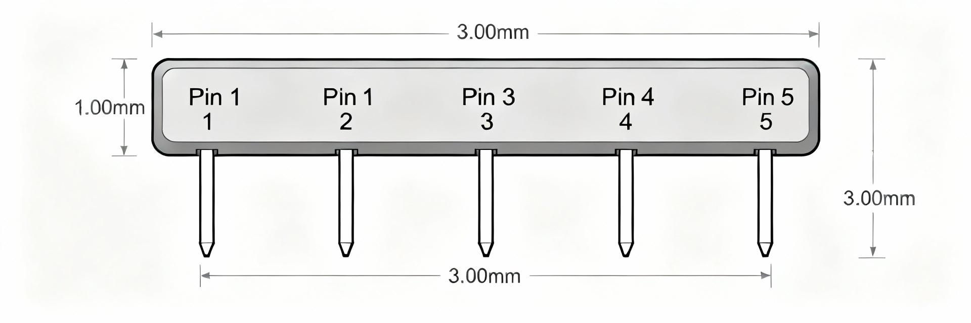
标题部分 3.00mm、5针通孔接头是混合电源和信号连接满足PCB鲁棒性要求的常见选择。本文为设计人员提供了简明的数据表、清晰的引脚输出和布局最佳实践。 介绍卡片 本指南承诺提供可操作的参考:紧凑的规格表、明确的引脚编号规则、三个示例引脚映射、PCB足迹建议、焊接和加固提示、替换清单、采购说明和故障排除步骤,以加快集成到生产中。 快速前部 快速规格和电气参数 关键电气规格 下方是一个适用于BOM和快速参考的紧凑型复制粘贴规格表。数值表示5针3.00mm穿心插座的典型、保守范围。 参数 典型 / 推荐 视觉评分 音高 3.00毫米(0.118英寸) 当前评级 典型每个触点2 A(1-3 A范围) 额定电压 高达250 V 绝缘电阻 > 1x10^9 Ω 典型 高可靠性 工作温度 −40 °C至+105 °C 工业级 引脚部分 引脚图和信号映射 引脚编号通常从组件侧带有护罩或凹口的端部开始,当从组件侧观察时,编号从最左侧的引脚开始,顶部朝上。始终通过PCB丝印层上的机械图纸和丝印参考进行验证。 映射卡1 示例 A:序列 + 功率 引脚1:VCC 引脚2:GND 引脚3:传输 引脚4:RX 引脚 5:NC 映射卡2 示例 B:I²C + 电源 引脚1:VCC 引脚2:GND 引脚3:SDA 引脚4:SCL 引脚 5:NC 地图卡3 示例C:5线传感器 引脚1:VCC 引脚2:GND 引脚3:DATA 引脚4:CLK 引脚5:警报 尺寸和占地面积 机械尺寸和占地面积 推荐PCB土地格局 钻头尺寸:Ø1.0–1.2 mm (表面贴装) 垫片直径:1.6–2.0 毫米 环状环≥0.5 mm 音高容忍度:±0.10毫米 专业设计师提示:在最终确定3D CAD之前,在机械图纸中考虑收割台护罩高度和栓钉位置。创建或导入3D STEP模型以检查配合间隙和附近的部件干涉。 组装最佳实践 安装、焊接与组装 焊接曲线 过孔选项包括波浪焊、选择性焊接或手动手工焊接。避免过度预热,并按照膏体规格保持峰值焊接温度。 机械支持 对于频繁的配合/不配合循环,添加机械加固:附近的安装孔,胶水圆角或额外的通孔连接到接地平面以获得刚性。 兼容性和替代方案 兼容性和替代品 拉代替清单: 确认3.00毫米间距 验证引脚数 (5) 检查电镀(金/锡) 对齐销钉存在 配置权衡: 移至2.54mm以增加密度 双排,引脚数更高 检查信号完整性 摘要部分 摘要 的0436500515规格表提供保守的电气参数和快速BOM输入的封装尺寸指导。 遵循pin1方向规则,在两端使用电源,在中心使用敏感信号,以获得最佳性能。 使用推荐的钻头/压板尺寸,并通过3D STEP模型验证,以确保生命周期可靠性。 常见问题手风琴区域 常见问题 什么是推荐0436500515通用异步收发设备和电源引脚?+ Recommended UART + power mapping places VCC and GND at pins 1 and 2 (ends) and TX/RX in the middle (pins 3 and 4), leaving pin 5 as NC or signal ground. This minimizes noise on data lines and simplifies cable routing. 我应该如何在我的 CAD 库中引用 5 针 3.00mm 头部焊盘?+ 包含钻孔尺寸、焊盘直径、环状环、丝印引脚-1标记和庭院层。为碰撞检查存储STEP模型,并为CAM提供推荐的焊盘布局。添加有关镀通孔要求的制造说明。 什么快速检查可以验证已安装的0436500515在第一篇文章检查期间?+ 检查针脚是否正确对齐,焊锡完全,没有焊锡桥,针脚1的正确方向,以及机械稳定性。对每个引脚进行导通测试,并在有限电流下进行通电烟雾测试。 Footer Meta 技术数据表集成指南 • 3.00mm 插针系列 •0436500515
2026-01-20 18:36:39