
Detailed analysis of I²t shifts and thermal derating across -55°C to +150°C for high-reliability PCB power rail protection.
Lab measurements and published time–current curves indicate that I²t and open time for the 0441005.WR can shift substantially across a typical −55°C to +150°C operating window—a critical concern for PCBs with high inrush or elevated ambient conditions. This report compares measured I²t behavior, quantifies temperature impacts, and provides practical test and design guidance for engineers specifying this SMD fuse.
The purpose is threefold:
Background: 0441005.WR SMD Fuse — Specs & Application Context
A compact, fast‑acting chip fuse rated for short‑circuit protection is commonly specified with the following nominal characteristics. Selection criteria must balance fault clearing energy versus allowed let‑through for downstream components.
Key Specifications at a Glance
| Parameter | Nominal Value (Datasheet Field) |
|---|---|
| Package | 0603 (Chip Fuse) |
| Rated Current | 5 A |
| Rated Voltage | 32 V |
| Speed Class | Fast‑acting |
| Operating Temperature | −55°C to +150°C |
| Rated I²t | Verify melt vs. arcing values |
Typical Use Cases & Design Constraints
- Constraint 1: Maximum expected inrush energy (I²t) must remain below fuse melt I²t with safety margin.
- Constraint 2: Continuous ambient/board temperature can reduce allowable let‑through energy — derating required.
- Constraint 3: PCB thermal mass and nearby heat sources dictate effective fuse temperature and behavior.
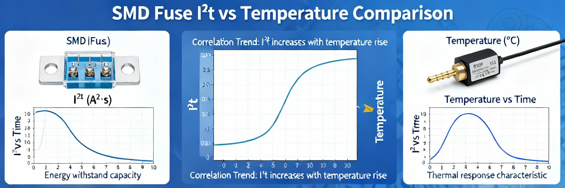
I²t Performance: Definition, Test Data Interpretation & Expected Curves
I²t Explained & Measured
I²t is the integral of I² over time (∫I² dt), representing let‑through thermal energy during clearing. Differentiate melting I²t (energy to melt the element) from arcing I²t (energy during sustained arc) when both values are reported.
Capture: ≥100 kS/s waveform sample rate. Units: A²·s.
Interpreting Measured Curves
Measured curves often deviate from datasheet graphs. Acceptable deviations depend on test fixture resistance, sample variability, and measurement method.
Temperature Limits & Thermal Derating
The stated operating range (-55°C to +150°C) describes survival, not guaranteed clearing consistency. Designers must consider local thermal rise on the PCB.
Conceptual I²t Derating vs. Temperature
*Interpolated data based on standard 0603 fast-acting fuse characteristics.
Test Methodology: Lab Setup for 0441005.WR
Required Equipment
- Programmable current source (fast slew rate).
- High-speed oscilloscope (100 kS/s minimum).
- Calibrated thermal chamber or hot plate.
- Low-inductance test leads and copper solder pads.
Procedure Best Practices
- Run baseline room-temp tests at multiple multiples of current.
- Measure at -40°C, 25°C, 85°C, and 125°C.
- Use ≥10 samples per condition for statistical mean/std dev.
Design Recommendations & Failure‑Mode Mitigations
Selection Checklist
If inrush exceeds margins, consider: NTC inrush limiters, slow-start circuits, or higher-I²t fuses. Avoid placing power-dissipating components immediately adjacent to the fuse.
Summary
I²t and temperature limits materially influence the suitability of the 0441005.WR for inrush‑heavy and high‑ambient designs. Engineers should extract datasheet melt/arcing fields, run controlled I²t vs. temperature sweeps, and apply a conservative 20–30% margin. The provided test methodology enables reproducible qualification and practical mitigations to reduce nuisance opens while maintaining protection.
Key Summary Points:
- Design margin ≥20–30% between inrush I²t and melt I²t.
- PCB thermal rise shortens time‑to‑open and reduces allowable I²t.
- Record raw waveforms at ≥100 kS/s for precise calculation.
- Mitigate via thermal layout, soft‑start, or NTC limiters.

