
在当前的功率转换和电机驱动设计中,隔离栅极驱动性能可以决定开关损耗和系统可靠性。证据:基准测试表明,具有>30 kV/µs CMTI和低于1µs传播延迟的栅极驱动光耦合器可以减少高dv/dt环境中的误触发。说明:本文提炼了ACPL-W340-500E数据手册对设计者所需的关键数字进行分析;这里出现了术语数据表,以标记来源上下文。
一点:我们的目标是实用的评估和一体化的指导。 证据:读者简明扼要的期望提取的输入/输出电器、隔离/CMTI、时间和热的限制。 说明:有针对性的外卖和表格,设计者可以图表数字门负责预算和布局限制之前,实验室验证。
背景:ACPL-W340-500E是什么以及它的适用范围
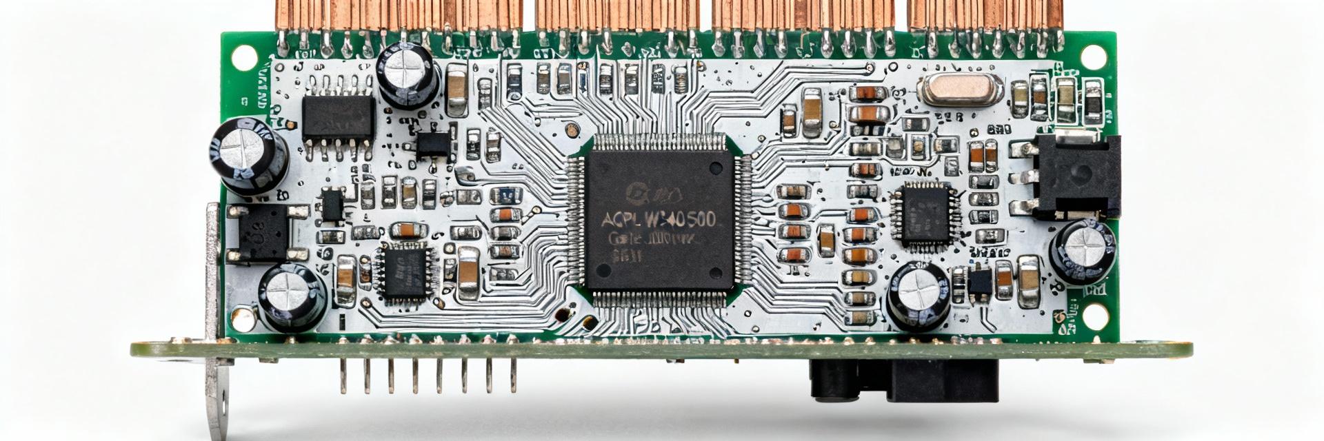
Device overview and package
Point: TheACPL-W340-500Eis an isolated gate-drive optocoupler with an integrated power output stage suitable for driving IGBT and power MOSFET gates. Evidence: The datasheet groups mechanical drawing, pinout and absolute maximum ratings in the initial sections for quick reference. Explanation: Designers should consult those sections for footprint, pin count and max stress limits before schematic capture and PCB land pattern creation.
目标应用和设计目标
典型的应用领域包括需要快速、强大隔离的电机驱动器、逆变器级和高功率电源。证据:该设备针对驱动电流、隔离和开关速度性能指标,这些指标对这些拓扑结构至关重要。说明:长尾查询,例如“ACPL-W340-500E门驱动的光电耦合器前"或"光电耦合器,用于精驱动器"反映实际的选择标准的工程师使用。
主要电气规格(数据表深度剖析)
Input (LED) electrical parameters to highlight
Point: Input LED specs determine required drive circuitry and input resistor when interfacing logic. Evidence: The datasheet lists DC forward current (If), forward voltage (Vf typ/max), input threshold and input power per channel under specified test conditions. Explanation: Use those values to size series resistors, to ensure the LED sees the correct current at your input logic voltage and to avoid overstress during fault conditions.
Output and supply-stage parameters to highlight
Point: Output capability governs achievable dV/dt control of gate charge and switching energy. Evidence: Extract output DC/peak current, output voltage range, saturation/drop, recommended VCC and typical load conditions from the datasheet tables. Explanation: Comparing typical vs. maximum values shows how much current is available for fast gate charging and how that translates to rise/fall times for a given gate charge.
| Parameter | Test Condition | Typical / Max |
|---|---|---|
| DC正向电流(如果) | DC,指定Ta | 如果评分,请参阅数据表 |
| 正向电压(Vf) | 如果 = 指定 mA | Vf typ / max |
| Input threshold | Specified test circuit | Threshold current / voltage |
Isolation, CMTI and Reliability Data (performance-critical metrics)
隔离额定值、爬电/间隙和测试条件
观点:隔离规格的保护,低压控制从高压电阶段。 证据:该数据表提供了额定电压隔离,隔离试验方法,和任何工作/加强绝缘注意到加推荐的PCB的爬/清除。 说明:设计人员必须映这些数字的系统一级的需求和强制执行最低PCB间隔、表面涂复的决定和对峙的间隙。
共模瞬态抗扰度(CMTI)和寿命/可靠性数据
观点:CMTI定义了对快速共模瞬态的免疫力,否则会导致误触发。证据:数据手册报告了带有明确测试条件的CMTI(kV/μs);列出最大质量限(MTBF)和工作温度范围以供可靠性规划使用。说明:使用数据手册中的CMTI和环境/工作温度规格来制定降额规则,并预测高dv/dt拓扑下的行为。
定时、开关和热性能(性能)
Timing and dynamic behavior
Point: Propagation delay and rise/fall times shape dead-time and shoot-through protection requirements. Evidence: The datasheet specifies propagation delay, rise/fall times and the test load circuits used to measure timing. Explanation: Designers should reference those test conditions when modeling dead-time margins and when sizing gate resistors to meet both switching-speed and EMI goals.
Thermal considerations and limits
Point: Thermal resistance and max junction temperature determine continuous operating capability under load. Evidence: The datasheet lists junction-to-ambient and junction-to-case thermal resistances plus maximum junction temperature and derating curves. Explanation: Implement PCB copper, decoupling and part placement strategies to keep junction temperature within safe limits when driving large gate charges repeatedly.
| Spec | 条件 | 注 |
|---|---|---|
| 峰值输出电流 | 脉冲测试 | Impacts gate charge slew |
| CMTI | Specified dv/dt test | High dv/dt immunity reduces false triggers |
| Propagation delay | 负载测量 | 用于死区计算 |
设计和集成指南(实用操作指南)
典型的栅极驱动电路和元件建议
参考电路将数据表编号转换为组件角色。证据:典型电路使用串联栅极电阻、下拉、钳位(TVS/缓冲器),有时还使用自举电源用于高侧驱动器。说明:使用输出电流和时序规格来选择栅极电阻,并决定给定MOSFET或IGBT栅极电荷是否需要主动米勒钳位或更强的下拉。
PCB布局、接地和EMI抑制技巧
要点:布局对于隔离、噪声控制和热性能至关重要。证据:数据手册中提到了爬电距离/电气间隙,并建议在VCC引脚附近进行去耦;实际规则包括分离噪声返回路径并最小化环路电感。解释:将去耦靠近器件放置,清晰布线返回路径,提供测试点,并在需要时使用专用隔离槽或涂覆层。
故障排除、比较和应用示例(可操作)
常见故障模式及调试清单
要点:常见问题包括无输出、驱动弱、误触发或热关断。证据:数据手册中的绝对最大值和时序/CMTI规格为测量提供了通过/失败阈值。解释:检查输入驱动电流、VCC电源轨、板卡间距,并通过受控的dv/dt测试确认CMTI裕量,以快速隔离根本原因。
示例应用场景和选择清单
要点:MOSFET的尺寸需要映射栅极电荷和开关频率以驱动能量和热预算。证据:使用数据表峰值输出电流和时序来计算开关期间的充电时间和平均功率耗损。说明:最终采购应根据实验室测试确认隔离额定值、CMTI、峰值输出电流和时序:开启/关闭波形、温升和隔离耐受测试。

