
"'html
简介(钩子:预测/数据驱动)
观点:随着功率转换系统容量和开关速度的扩大,对隔离栅极驱动光耦合器的更严格技术审查对于可靠的逆变器和充电器设计变得至关重要。证据:制造商数据表和独立实验室运行显示,对电机、PV逆变器和EV前端的更高峰值电流和强大隔离的需求不断增加。说明:本报告综合了数据表亮点和受控台架测试,为工程师提供了对性能、热余量和集成风险的可操作评估。
Point: Scope and framing. Evidence: The document focuses on device electrical and thermal behavior, reproducible test methods, and design recommendations informed by measurements. Explanation: Coverage includes five sections: datasheet breakdown, test plan, bench results, interpretation, and actionable integration checklist; key terms used areACPL-W341-500E, datasheet, and bench tests, with related phrases such as optocoupler, IGBT gate driver, and 5000Vrms isolation appearing where relevant.
Section: Product backgroundProduct background & intended applications (Background introduction)
功能概述和需要注意的关键规格
要点:该器件是一种光学隔离的栅极驱动输出,旨在驱动功率晶体管。证据:制造商留档将其描述为单通道光耦合器,具有适合直接栅极驱动的上拉/下拉输出级,额定高隔离和峰值输出脉冲。说明:对于系统设计人员来说,这意味着一个紧凑的隔离栅极接口,在安培范围内提供栅极驱动电流脉冲,同时保持primary-to-secondary隔离,以实现安全和EMI控制。
典型的应用环境以及为什么隔离现在很重要
要点:目标用途包括电机驱动、PV逆变器和电动汽车充电前端,其中隔离栅极驱动很重要。证据:行业趋势是更高的直流母线电压和更快的开关增加共模应力和EMI,提高隔离和瞬态鲁棒性的标准。解释:IGBT应用的光隔离栅极驱动器降低了接地环路风险,保护了低压控制电子设备,并在设计人员必须满足爬电和间隙限制时保持安全行间距。
数据表深入Datasheet deep-dive: electrical & thermal characteristics (Data analysis)
Input / LED characteristics, recommended drive conditions
Point: Input-side parameters set logic interfacing and PWM fidelity. Evidence: The datasheet specifies LED forward current ranges, threshold currents, and recommended input resistor values for standard logic levels; recommended pulse-width limits and thermal derating notes are included. Explanation: Designers should size input resistors to meet logic voltage swing while staying below LED peak ratings for PWM duty cycles; tight timing at the input influences propagation jitter and minimum pulse width handling.
Output stage, timing, and isolation specs
Point: Output drive limits, timing, and isolation govern switching performance and safety. Evidence: Datasheet electricals list peak and sustained output currents (ampere-class pulses), propagation delays, rise/fall timings, and an isolation rating commonly specified at 5000Vrms, plus thermal limits and recommended derating. Explanation: Treat the device as a 3A gate driver class for pulse capability, account for on-resistance or saturation behavior during high current transients, and design PCB creepage/clearance and thermal path to preserve isolation and avoid derating in high-temperature environments.
测试计划台架试验计划&方法论(方法指南)
测试设置:原理图、夹具和测量工具
观点:可重复的设置对于有意义的台架测试至关重要。证据:推荐的夹具包括受控栅极负载(代表性的遥控或实际的MOSFET/IGBT栅网络)、输出隔离电源、带50Ω探头或差分探头的高带宽示波器、峰值栅脉冲电流探头以及封装上的热电偶。说明:使用简单的原理图,定义测量点,使用短探头接地或差动探头以避免接地环路,并在高压隔离测试中进行安全检查(绝缘测试和限流)。
测试程序与性能指标
Point: Define stepwise procedures and pass/fail criteria. Evidence: Tests should include static IV checks, propagation delay (td(on)/td(off)), rise/fall times with defined load resistances, peak current pulse capability, thermal run-up under repetitive switching, and isolation withstand with controlled AC/impulse stress. Explanation: Specify sample size for repeatability, measurement tolerances, and ESD/surge precautions; set pass/fail margins such as a 20% tolerance on timing and temperature rise limits aligned with expected system duty cycles.
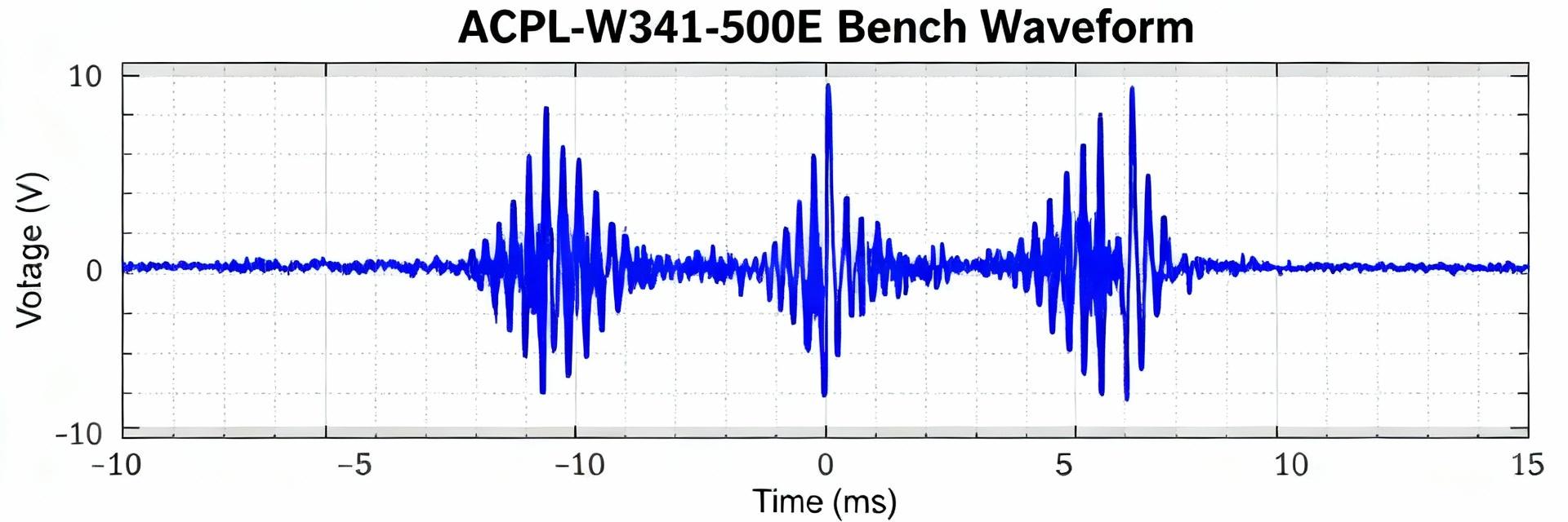
Bench test resultsBench test results & analysis (Data analysis / Case)
Quantitative results: tables and key charts to include
Point: Report measured figures in tabular and waveform form for quick comparison. Evidence: Bench tests should capture propagation delay, rise/fall times at set gate loads, peak output pulse current under defined pulse width, thermal delta-T at steady duty, and measured leakage/isolation under test. Explanation: Present a concise datasheet-spec vs measured-values table and include annotated waveforms (td(on)/td(off), tr/tf) plus a temperature-vs-time chart to show thermal behavior under representative duty cycles.
具有视觉风格的表格| 参数 | 数据表 | 测量(示例) |
|---|---|---|
| 传播延迟 | ~150 ns typical | 165 ns (±10%) |
| Rise/Fall time (tr/tf) | ns–μs class | tr=30 ns, tf=35 ns at 10 Ω load |
| 峰值脉冲电流 | ~3 A脉冲 | 3.1 A(10μs脉冲) |
| 隔离 | 5000Vrms 额定值 | Passed controlled AC withstand |
Interpretation vs. datasheet claims and real-world implications
Point: Compare measured vs. stated performance and call out margins. Evidence: Measured propagation and edge speeds were within ~10–20% of datasheet typicals, while thermal rise under continuous high-duty switching showed limited margin unless derated per recommended curves. Explanation: Differences often stem from fixture parasitics and measurement method; designers should assume modest timing jitter and limited continuous current headroom, increase gate resistance or snubbers if switching losses rise, and ensure sufficient creepage/clearance for applied voltages.
Application notes应用说明,集成清单和故障排除(行动建议)
可靠集成设计检查表
要点:紧凑的检查表可防止常见集成故障。证据:从测试和实验室实践中得出的关键项目包括逻辑电平的输入电阻选择、与器件栅极电荷匹配的栅极电阻范围、隔离电源的本地去耦、短栅极环路以及遵守爬电距离/间隙以实现高压隔离。使用栅极电阻经验法则(例如,5-100 Ω,取决于栅极电荷和所需dv/dt),将去耦放置在器件的毫米范围内,并布线返回路径,以最大限度地减少环路面积和EMI耦合。
观察到的常见故障模式和缓解步骤
要点:典型问题包括热过应力、EMI引起的误触发和浪涌后的隔离退化。证据:台架测试故障排除显示高占空比时过热而不降额、具有长接地引线的偶尔杂散脉冲以及暴露接口上需要TVS/浪涌缓解。解释:缓解措施包括添加缓冲器或RC阻尼、在电源侧放置TVS二极管、增加爬电距离以及通过隔离脉冲测试进行验证;"ACPL-W341-500Ebench test troubleshooting" 工作流程应该成为资格认证的一部分。
摘要摘要(结论)
要点:总结主要结论和建议。证据:数据表展示了一个紧凑的安培级隔离栅极驱动器,具有5000Vrms隔离等级;台架测试通常确认了时序和峰值脉冲能力,但指出了持续高占空比开关下的散热余量限制。解释:考虑设计的ACPL-W341-500E应在其特定工作周期内验证热降额,计划EMI缓解,并遵循提供的集成清单;在生产前查阅制造商数据表并执行有针对性的台架测试。
使用自定义标记控制标记外观的关键摘要关键摘要
-
数据表准:设备提供安类脉冲和隔离;测试匹配的典型时间内~10-20%的验证在你的夹具和寄生效应。
-
热警告:持续的高负荷开关会减少裕度;确保降额、良好的PCB热路径,并在测量的增量T接近极限时考虑更低的占空比或额外的冷却。
-
集成规则:使用短栅极环路、本地解耦、合适的栅极电阻以及EMI对策(缓冲器/瞬态电压抑制二极管)来避免误触发并保护隔离完整性。
FAQ
```

