
要点:SI 8235 BB是一款双通道隔离式栅极驱动器,额定峰值驱动电流约为4 A,隔离度约为2.5 kVrms,这些数据表明它适用于中高压功率级。证据:这些峰值电流和隔离度数字定义了驱动器对栅极电容充电/放电的速度以及它支持的隔离范围。本文将这些转换值转换为可测量的板载性能、布局动作和热现实,以便设计人员能够预测真实的转换器和电机逆变器的行为。
背景:为什么隔离式栅极驱动器在现代电力系统中很重要
隔离、安全和监管环境
要点:电流隔离保护低压控制免受高压电源的影响,并支持法规爬电/间隙要求。证据:接近2.5 kVrms的隔离额定值表明强大的介电耐受能力,并有助于设置工作电压等级和PCB爬电行间距。解释:设计人员通过根据目标工作电压和污染程度选择爬电/间隙、放置屏障轨道和适当开槽来将隔离额定值映射到系统绝缘,以便隔离栅极驱动器满足系统安全和浪涌预期。
典型拓扑结构和功能角色
Point: Isolated gate drivers are used for half-bridges, full bridges and high-side gate drive where bootstrapping is inadequate or multi-level isolation is preferred. Evidence: dual-channel isolation consolidates two gate drives into one package, simplifying board routing and ensuring matched timing between channels. Explanation: In converters driving Si, SiC or GaN switches, a dual isolated driver reduces component count and eases layout in multiphase or bridged topologies while providing independent isolated supplies and balanced propagation behavior.
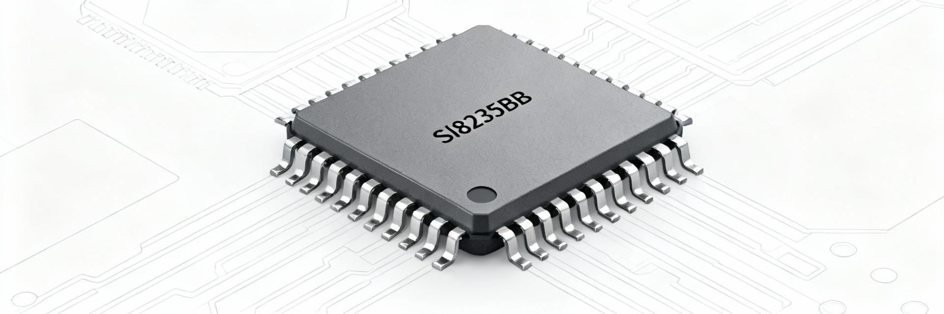
SI8235BB performance specifications overview
Key electrical specs to benchmark
Point: Engineers should benchmark peak output current (4 A peak), propagation delay, input-to-output isolation voltage, common-mode transient immunity (CMTI), UVLO thresholds, gate voltage swing and output fault behavior. Evidence: peak drive current governs how fast gate charge is delivered; propagation delay and skew determine timing margins; CMTI quantifies immunity to high dv/dt events. Explanation: Tracking these metrics during validation links switching losses, timing margins and transient immunity to observed device stress—enabling safe switching-environment specification and coordinated gate resistor selection.
Thermal, SOA and reliability considerations
观点:峰值电流额定不等于连续能力;热降额和封装热阻定义了安全连续运行。证据:高重复率驱动单元脉冲会产生平均功率,必须通过PCB铜、通孔和对流去除;SOA极限可能在峰值规格应力之前就已达到。说明:通过计算每次开关事件的能量、给定开关频率和占空比的平均功率,将峰值电流能力转换为实用连续驱动,然后利用PCB热路径和降额曲线设定最大可持续栅极驱动活动。
可视化报表/CSS图表表示快速可视化指标
Notes: bar widths are relative visual indicators for quick comparison; validate against full datasheet graphs for precise thermal/SOA limits.
SI8235BB实验室测试与实际性能
推荐的测试设置和测量程序
要点:精确的测量需要仔细的探测、受控的解耦和安全的隔离实践。证据:使用短接地线或隔离探头作为回路,将高频去耦电容器放置在电源引脚毫米范围内,并在高压测试期间保持隔离,保持适当的夹具间隙。说明:推荐程序:将DUT安装在代表性PCB上,用通孔缝合接地,将示波器探头接地作为弹簧或使用有源探头,测量代表性栅极电荷负载下的上升/下降时间、传播延迟和峰值电流,同时监测驱动器温度和隔离完整性。
解释结果和常见故障模式
点:与数据手册数值的偏差指向布局或供电问题;常见故障包括假切换、热折回和锁存。证据:边缘速度低于预期通常源于过大的环电感或解耦不足;CMTI失效与共模dv/dt较大以及屏蔽不足相关。解释:当观察到的升降时间较长时,检查门环区域和解耦;如果在高DV/DT期间出现杂乱切换,应添加局部共模滤波,提高栅极电阻或改善隔离布线,并重新测试可靠性。
Comparative scenarios & application case studies
High-frequency wide-bandgap converter scenario
Point: Driving SiC/GaN at high dv/dt amplifies demands on timing, CMTI and gate-charge delivery. Evidence: faster edges lower switching loss but raise EMI and stress the driver and transistor; repeated fast pulses increase average driver dissipation. Explanation: Quantify trade-offs by measuring switching loss vs. EMI at multiple gate resistor values, ensure CMTI margins exceed expected dv/dt, and size thermal path and decoupling so the gate driver maintains specified rise/fall times without thermal throttling at the target switching frequency.
Motor drive / inverter scenario
Point: Continuous operation in motor inverters emphasizes thermal management and deadtime control. Evidence: bootstrapped supplies may be convenient for low-side drivers, but multiphase systems benefit from isolated supplies to avoid bootstrap recharge complications. Explanation: A dual isolated gate driver simplifies multi-phase layouts by providing matched channels; designers should tune deadtime to prevent cross-conduction, monitor continuous junction temperatures, and verify long-term reliability under expected ambient and load conditions.
最佳性能的设计检查表和优化提示
PCB布局、解耦和EMI缓解
地点:布局和优先耦产生最好的测量的上升或下降时间和减少冲。 证据:地方去耦盖邻近的驱动程序VCC针,利用开尔文的路由栅返回,并尽量减少栅源循环的区域减少感性冲。 解释:逐步清单—1)短期、广泛的权力循环,与固的铜倒;2)当地高频耦和散装储库;3)专门的返回通路和Kelvin门跟踪;4)地方栅阻靠近驱动的产出;5)加入缓冲器或RC阻尼控制的铃声。
热管理和降额指南
要点:平衡栅极电阻选择和铜散热,以管理开关损耗并限制驱动器温升。证据:较低的栅极电阻会加速边缘,但会提高峰值di/dt和EMI;较大的铜面积和热通孔会降低驱动器结温。解释:经验法则:对于中等频率的硅MOSFET,从5-20Ω开始;对于高频的SiC/GaN,考虑1-10Ω,具有更强的热缓解;始终通过测量驱动器外壳温度并相应地调整电阻和铜来验证。
Summary
-
The dual-channel isolated gate driver delivers strong transient drive and robust isolation; real-world performance hinges on layout, decoupling, and thermal strategy and must be validated under representative gate-charge and dv/dt conditions.
-
Benchmark key specs—peak current, propagation delay, CMTI and isolation voltage—using a controlled test fixture; interpret deviations as layout, decoupling or supply issues and iterate accordingly.
-
Prioritize thermal paths, gate resistance tuning and EMI controls early in design: follow the measurement procedures, apply the layout checklist, and perform thermal and CMTI verification prior to system integration.