
的LPC802M001JDH20Jis a purpose-built, ultra-compact 32-bit Cortex-M0+ MCU family member optimized for low‑power embedded designs; it advertises a maximum CPU clock of around 15 MHz, an entry‑level flash footprint, multi‑channel ADC and common serial interfaces. This introduction frames what the part actually delivers for US product and prototype workflows and points engineers toward the official datasheet for final verification.
Practical use favors tiny battery‑powered nodes, low‑cost consumer controls and compact sensor endpoints where package size and power dominate decisions. Read the official datasheet revision and errata before design lock: focus first on electrical characteristics, memory map and pinout to verify the exact specs for your chosen variant.
Why the LPC802M001JDH20J matters (background)
Target applications and product fit
Point: The MCU is aimed at minimal‑function, cost‑sensitive embedded products. Evidence: Typical fits include simple sensors, basic control nodes and battery‑powered IoT endpoints where MCU functions are modest. Explanation: Designers trade off raw compute and feature set for low BOM cost, small PCB area and low quiescent current—making this part a sensible choice for multi‑year battery targets and compact consumer devices.
官方数据表和修订说明
要点:始终查阅官方数据表PDF和当前勘误表。证据:数据表包含决定板级决策的电气表、内存映射和引脚描述。解释:从制造商网站或授权留档门户获取数据表,检查文档修订和勘误表ID,并首先读取电气特性、内存映射和引脚输出页面,以在印刷电路板布局之前捕获封装变体和绝对最大值。
LPC802M001JDH20J:关键电气和内存规格(数据深度挖掘)
Core, clock and voltage specs
Point: Cortex‑M0+ core with modest maximum clock and a single‑supply domain suits low‑power designs. Evidence: The part targets a maximum CPU clock around 15 MHz with standard internal oscillator options and a single‑supply operating window typical for low‑voltage MCUs. Explanation: Clock and supply choices directly affect performance and current draw—lower clock and reduced core voltage yield proportional savings in active current, so configure clocks only as high as needed for the workload to maximize battery life.
Memory and storage layout
Point: Memory is sized for compact applications. Evidence: This family is an entry‑level flash class (typical devices in this family sit in the ~16 KB flash region) with a small SRAM block sufficient for lightweight stacks and buffers; boot ROM features often provide a minimal bootloader. Explanation: Flash and RAM limits constrain large frameworks and over‑the‑air images; keep firmware lean, use link‑time garbage elimination, and verify the exact flash/RAM numbers in the datasheet before committing to production.
LPC802M001JDH20J peripherals & interfaces breakdown (data deep‑dive)
模拟外设:ADC和比较器
要点:片上模拟支持基本传感。证据:期待10-12位级别的多通道ADC,具有可选的参考选项和少数适合温度、光和电池传感的通道。解释:ADC采样策略很重要——使用平均、适当的参考选择和输入调节来满足测量精度,而不会增加固件复杂性或功耗。
数字接口:I2C、SPI、USART、定时器、GPIO
要点:MCU公开了常见嵌入式任务的基本串行和定时器外围设备。证据:典型的产品包括I2C、SPI和至少一个USART、具有PWM功能的基本定时器和具有引脚多路复用约束的GPIO;入门级设备通常不存在或限制DMA。解释:多路复用引脚需要规划——映射传感器和调试引脚以避免冲突,以及围绕单主SPI/I2C突发而不是高带宽流的预算吞吐量期望。
性能、功耗和热极限(数据分析)
Power modes, current draw and battery planning
Point: Power profiles determine battery life more than peak CPU speed. Evidence: Typical devices show low‑microamp deep‑sleep and modest active currents at low MHz; a simple battery‑life calculation uses average current = duty%*active_current + (1-duty%)*sleep_current. Explanation: Example: with 1% active duty, 5 mA active peaks and 5 µA sleep, average current ≈55 µA; a 2,000 mAh cell yields ~36,000 hours (~4 years) of theoretical life—use datasheet figures for accurate planning and include radio or sensor currents if present.
Small visual bar chart (CSS via inline styles)5 mA
0.005毫安
0.055 mA
Thermal, package and operating conditions
Point: Small packages limit thermal dissipation and continuous high‑current operation. Evidence: The part is available in compact 20‑pin small‑outline packages with standard commercial temperature ranges; continuous high‑power draw forces derating. Explanation: For sustained loads, follow the datasheet thermal guidance, avoid heating from nearby regulators or radios, and design for the worst‑case ambient to keep junction temperature within limits for reliable lifetime.
Hardware integration & PCB guidelines (method guide)
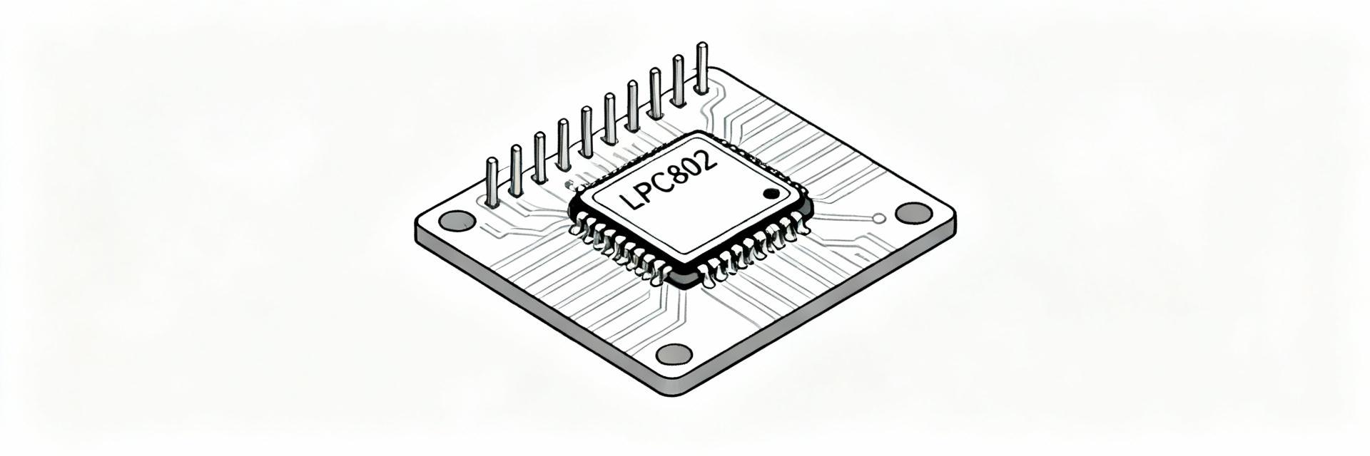
引脚、包装选项和占地面积提示
要点:正确的占用空间和引脚分配可以防止返工。证据:关键引脚包括20引脚引脚中的VDD、VSS、RESET和调试线(SWDIO/SWCLK);小封装限制路由和解耦放置。解释:在VDD引脚附近放置一个初级0.1μF解耦电容器,保持RESET和调试痕迹较短,并在MCU下保留接地浇注,以稳定返回路径并降低EMI。
电源、时钟和复位电路建议
要点:简单的电源和复位电路提高了可靠性。证据:在VDD上使用0.1μF陶瓷去耦加1μF体积帽,在RESET(10 kΩ)上拉,如果使用施密特触发器输入进行外部复位。解释:如果需要外部振荡器,请遵循晶体或振荡器模块的布局指南;否则使用带校准的内部RC,以减少组件数量和电路板面积。
固件、编程和开发工作流程(方法指南)
Bootloader, debug and programming interfaces
Point: Multiple programming paths simplify prototyping. Evidence: Devices typically provide a ROM boot path and SWD debug interface; flashing is possible with a standard SWD‑compatible tool using SWDIO/SWCLK plus VDD/GND and optional RESET. Explanation: During prototyping, keep SWD accessible and plan for a production debug header or programming pogo pad; verify minimal signals needed from the datasheet before wiring fixtures.
Minimal BSP & example start‑up sequence
Point: A compact startup saves flash and RAM. Evidence: Minimal init includes oscillator setup, GPIO defaults, ADC calibration and low‑power configuration. Explanation: Initialize clocks to the lowest frequency that meets timing, set unused pins to defined low‑power states, sample ADC only when needed, and use link‑time optimization and stripped C libraries to minimize footprint.
Application examples & design checklist (case + action suggestions)
3个简洁的示例项目
示例1:电池环境传感器-外围设备:ADC、I2C温度/湿度、低功耗定时器;预期内存:小型引导加载程序+紧凑传感器堆栈(~8-16KB闪存);电源:周期性唤醒、采样、传输、深度睡眠策略。示例2:简单的电机/触觉控制-外围设备: PWM定时器、GPIO、小型状态机;内存:用于输入防抖和控制的适度固件。示例3:通用步异收发设备/I2C桥接-外围设备:USART和I2C,最小缓冲;内存和CPU足以实现低吞吐量桥接。
设计和采购清单
要点:在订购前确认变体细节。证据:第一个清单项目:获取官方数据表,并验证您计划购买的包装变体的确切零件标记、修订和详细规格。解释:还要确认包装类型、编程/调试适配器兼容性、订购样品以进行布局验证,并确保生产数量的供应连续性。
总结
-
TheLPC802M001JDH20Jis a compact, cost‑focused Cortex‑M0+ option for tiny, low‑power embedded designs; verify flash/RAM and electrical numbers in the official datasheet before committing.
-
Plan power early: use low duty cycles, minimal clocks, and accurate battery‑life calculations based on datasheet current figures.
-
Prototype with SWD debug access, correct decoupling and pin‑mux planning to catch layout issues before production.

