
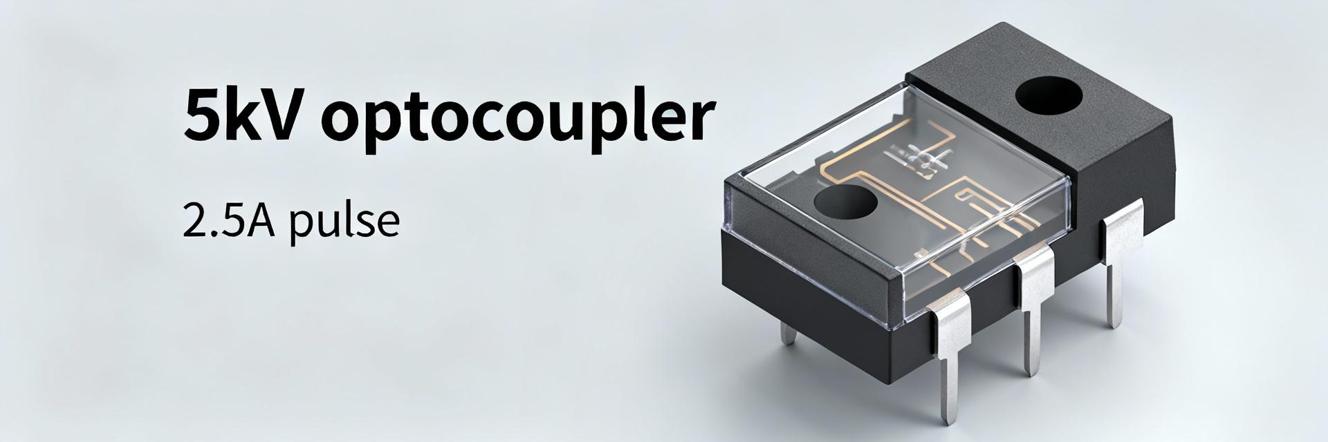
该器件将高隔离、快速开关和强峰值驱动相结合。证据:额定5 kVrms隔离、~2.5 A峰值输出能力和低于25 ns的上升/下降行为。说明:本文对光耦合器及其隔离栅极驱动和控制接口的实际性能进行了实用的、以测试为导向的检查。
背景:为什么这种光耦合器对于隔离式栅极驱动器很重要(背景介绍)
Core function & target applications
Point: An optocoupler isolates low-voltage control from high-voltage power stages. Evidence: used in motor drives, inverters, industrial controls and telecom interfaces to transfer logic signals across safety barriers. Explanation: isolation prevents ground loops and protects controllers while allowing gate-drive signaling; designers prioritize isolation rating, drive capability and switching speed for reliable operation.
Isolation concepts & system-level implications
Point: Isolation rating affects PCB spacing and safety margins. Evidence: creepage/clearance rules and working vs. isolation voltage determine required keep-out and surge margins. Explanation: a 5 kVrms isolation rating raises allowable transient headroom, but designers must translate that into PCB creepage distances, insulation materials and decision points for spacing and conformal coating.
ACPL-K342-500E: Datasheet highlights & what each spec means (Data analysis / Specs)
电气和LED特性(输入)
要点:输入LED参数设置控制器的驱动要求证据:关键值包括最大正向电流、典型正向电压和CTR或输入到输出耦合建议说明:实用设计使用MCU或电平移位器输出,从Vf和所需的If中选择串联电阻,并尊重输入时序限制,以避免脉冲操作期间的热应力。
输出、隔离和时序规格(输出)
输出规格决定开关性能和安全操作区域。证据:亮点数字包括约2.5 A的峰值输出、5 kVrms隔离和22 ns附近的上升/下降时间以及传播延迟和热极限。说明:峰值驱动器支持快速门充电;上升/下降时间和传播延迟控制开关损耗和时序裕度;高占空比或重复脉冲需要热降额。
用于可视化数值规格的内联CSS条形图性能基准和测试驱动的见解(数据分析/性能)
推荐实验室测试和预期结果
要点:短台架测试套件验证数据表声明。证据:使用定义的CL/RL捕获开关波形,在热监控下测量上升/下降、传播延迟和脉冲输出电流。解释:预期基准包括轻负载下低于25 ns的边缘和经过验证的2.5 A短脉冲;记录公差并在升高的环境下重复测试,以暴露降额行为。
Robustness: ESD, surge and failure modes to watch
Point: Stress tests reveal common failure mechanisms. Evidence: overcurrent pulses, high dV/dt on outputs and sustained heating are typical stressors. Explanation: interpret outcomes by noting output saturation, timing shifts or permanent LED degradation; mitigate with series resistors, snubbers, current-limiting and improved heat spreading to prevent cumulative damage.
Design & integration guide: PCB, layout and circuit tips (Method / How-to)
PCB layout, creepage/clearance and grounding practices
Point: Layout enforces the isolation rating and signal integrity. Evidence: keep the isolation barrier free of copper, route low-inductance returns, and use stitching vias for safety ground zones. Explanation: set minimum keep-out, label silkscreen warnings, employ solder mask over slots where needed, and place input-side components away from high-voltage conductors to minimize coupling and improve testability.
栅极驱动电路示例及无源元件推荐
要点:外部元件定制驱动强度和阻尼。证据:典型模式使用从Vf和If大小的串联输入电阻,输出上拉/下拉和栅极电阻用于MOSFET/IGBT开关。说明:选择缓冲RC进行dv/dt控制,调整栅极电阻以交换开关速度与过冲,并考虑SO-8/SOIC处理功率脉冲场景中的封装热限制。
比较和用例场景(案例研究/情境化)
权衡对其他的隔离的方法
点:光耦合器将速度和简单性与一些集成隔离替代品进行交换。证据:基于光耦合器的驱动器紧凑、经济实惠且易于路由,但需要仔细布局以满足更高速度的需求。说明:与变压器或电容隔离器相比,它们通常更适合中速栅极驱动器,其中简单性和峰值驱动最为重要。
Example application profiles
Point: Three short profiles show practical priorities. Evidence: (1) Three-phase motor inverter gate-drive needs fast edges and thermal margin; (2) industrial relay isolation emphasizes robustness and surge tolerance; (3) MCU-to-high-voltage sensor interface values creepage and noise immunity. Explanation: list top design considerations: switching losses, surge handling, and isolation spacing respectively.
Buyer's checklist & next steps for validation (Actionable recommendations)
Pre-purchase checklist
Point: Confirm mechanical, electrical and compliance fit before procurement. Evidence: verify package type/pitch, required isolation rating, supported output pulse currents, operating temperature range and generic safety certifications. Explanation: obtain samples for lot-to-lot checks, request recommended land pattern and reflow profile, and ensure procurement includes sample testing plans.
产品发布前的验证计划
要点:验收测试可降低现场风险。证据:验收包括电气台架测试、热循环、隔离耐受性和基本EMC评估。解释:运行可重复的测试序列,在压力下记录传播/定时偏移,并编译数据表、着陆模式和应用说明,作为产品发版最终签字留档的一部分。
结论(摘要和SEO)
要点:该器件将高隔离性与有意义的峰值驱动和栅极驱动使用的快速开关相结合。证据:额定5 kVrms隔离、强大的脉冲输出能力和快速边缘支持苛刻的接口。说明:只有通过深思熟虑的PCB布局、组件选择和台架验证来确认系统内行为,才能实现预期的性能。
关键的摘要
-
▸
高隔离度与强脉冲驱动:设备提供较高的瞬态裕量,以及约2.5A的峰值能力用于短栅极电荷事件;设计人员必须将隔离等级转化为PCB间距和绝缘实践。
-
▸
速度与热能权衡:小于25纳秒的边缘可以实现快速切换,但会增加切换损耗;热能降额和脉冲电流限制应指导布局中的占空比和散热选择。
-
▸
测试驱动的验证要求:执行波形捕获、传播延迟和脉冲的电流试验加上隔离承受和热骑自行车,以确认实世界中的表现之前生产。

